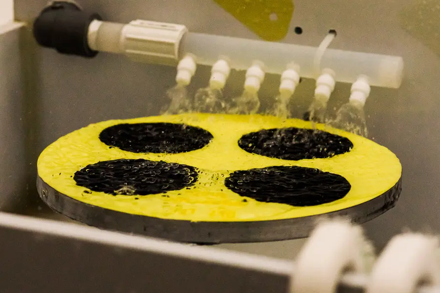
Bigger isn't automatically better when choosing a silicon wafer diameter. The right size depends on what the wafer actually needs to do, and defaulting to the largest option available can mean paying for capacity a project will never use.
Our own silicon wafer options page lists the diameters available. Still, the harder question is which one actually fits your process.
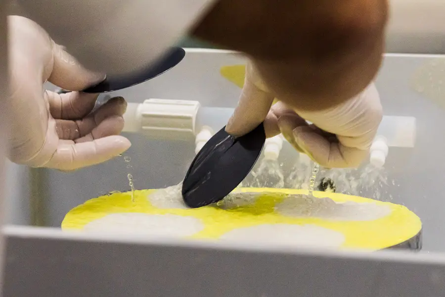
Diameter is not just a size preference; it is a compatibility requirement. According to SEMI, the global standards body for the semiconductor industry, wafer specifications from 50mm to 450mm exist specifically to ensure that equipment across different fabs and suppliers remains interchangeable.
A fab tooled for one diameter generally cannot process a different one without new equipment, making diameter one of the first constraints to check.
Smaller diameters, from 2-inch up through 100mm, tend to make more sense for research, prototyping, and low-volume specialty work. Universities, government labs, and early-stage device development rarely need the volume that larger wafers are built to support, and smaller diameters keep upfront costs down without requiring bulk ordering.
Our guide to the full range of standard diameters covers where each size is typically used across different applications.
Larger diameters, mainly 200mm and 300mm, dominate high-volume silicon wafer production because they reduce the cost per die, even though the wafer itself costs more. More usable surface area means more chips per wafer, which is the entire economic argument behind the industry's shift toward larger sizes over the past several decades.
Our deeper comparison of 200mm, 300mm, and 450mm wafers breaks down how that math actually plays out.
A few questions tend to clarify which diameter actually fits a given project.
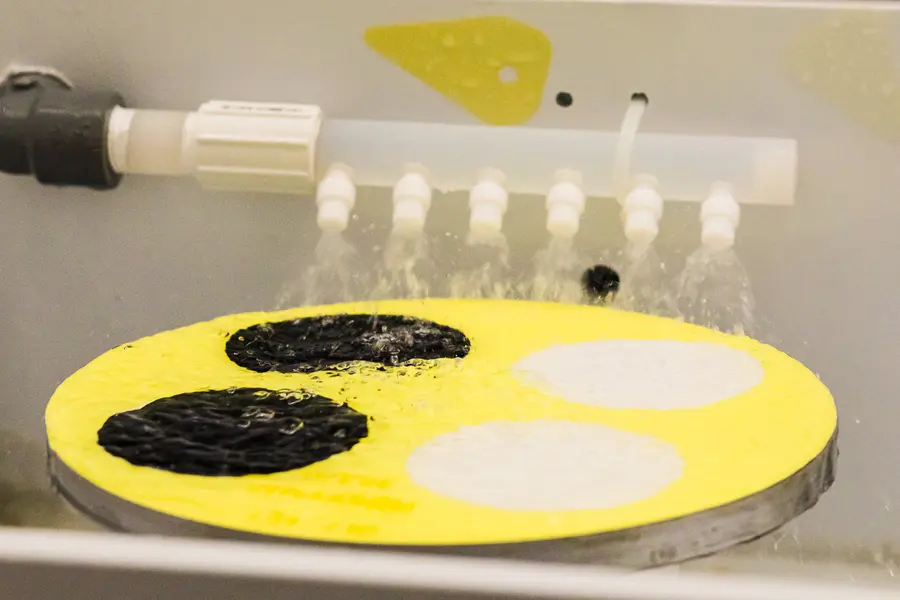
Specifications, tooling constraints, and volume needs all factor into the decision, and getting it wrong upfront is expensive to correct later. Wafer World can help match your specific application to the right silicon wafer diameter and specs before you order.
Request a quote to talk through your project requirements with our team.




