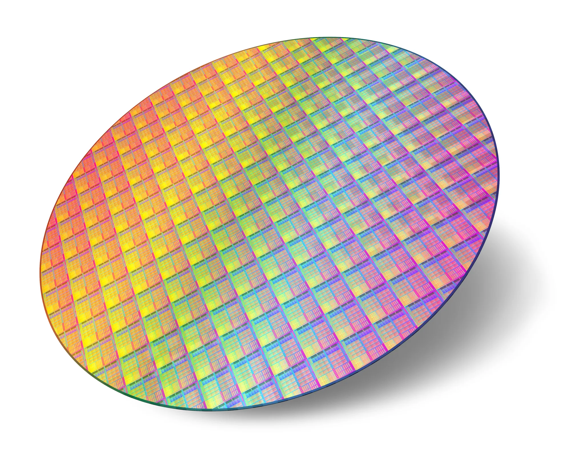
A wafer is a thin slice of semiconductor material, such as a crystalline silicon, used in electronics for the fabrication of integrated circuits and in photovoltaics for conventional, wafer-based solar cells. The wafer serves as the substrate for microelectronic devices built in and over the wafer. Let’s take a look at some of the common silicon wafer related terms.
Adhesion - the ability of materials to stick (adhere) to each other.
Boron - element from group III of the periodic table; acts as an acceptor in silicon; Boron is the only p-type dopant used in silicon device manufacturing.
Cleanroom - enclosed ultra-clean space necessary for semiconductor manufacturing. Airborne particles are removed from the space to specified minimum levels, room temperature and humidity are strictly controlled.
Compound Semiconductor - synthetic semiconductor formed using two or more elements mainly from groups II through VI of the periodic table.
Diffusion Pump - high vacuum pump operating in the ranges from 10-3 torr to 10-7 torr featuring relatively high pumping speed.
Ingot - circular piece of single-crystal semiconductor material resulting from a crystal growth process.
Reclaim Grade - A lower quality wafer that has been used in manufacturing and then reclaimed (etched or polished) and subsequently used a second time in manufacturing.Slicing - the term refers to the process of cutting of the single-crystal ingot into wafers.
Wafer Bonding - a process in which two semiconductor wafers are bonded to form a single substrate.
If you are looking for silicon wafers, look no further than wafer world. Contact us today to learn more about how we can help you with all your wafer needs.


