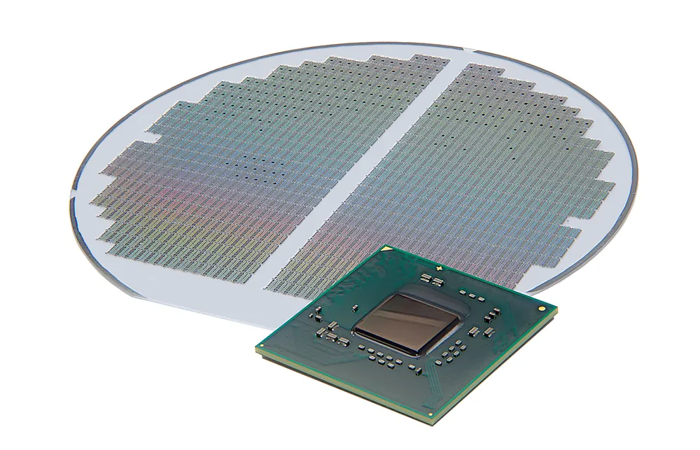
Silicon wafer suppliers know that, in order for the wafer to be useful, it must have little to no defect. Wafer defects range from holes and micro-scratches on the surface to flaws concealed in the silicon bulk. If you are planning to buy silicon wafer for your business or for your next project, here are the common wafer defects you need to be aware of certain defects.
Mixed dislocation- a combination of both edge and screw dislocation.
Screw dislocation
Plane/ Area Defects
Twin Boundaries
Stacking Faults
Grain Boundaries- this is the development or juncture between crystals whose atomic composition deviate in orientation with respect to each other.
Volume or Bulk Defects
Precipitates of external and internal point flaws.
Voids
Stacking Faults and Twins
This defect is common in III-V semiconductor crystals. Stacking defects is a flaw in the stacking series of atomic planes in the crystal mesh. A twin shows two areas in the crystal with one area a mirror reflection of the other across a twin plane that is shared in both areas.
Point Defects
Include foreign atoms, vacancies, antisite defects, and interstitials. Electrical properties and concentration of point defects are controlled by Melt stoichiometry.
Dislocations
Dislocations originate from three mechanisms during bulk crystal growth.
The Three Mechanisms Are:
Non-uniform heat flow during hardening that results in thermal stress.
Condensation of excess point defects producing displacement coils.
Propagation of dislocations from damaged seed crystal from external particles or inclusions.
Specifications Affecting Dislocation Density:
Crystal Diameter
Melt stoichiometry
Cone Angle
Seed quality and necking
Ambient pressure
What is Twinning?
Twinning is a Result of the Following:
Too much facet formation
Nucleation at the crucible wall
Thermal breakdown following growth
Imbalance in the shape of the crystal growth front
Change from melt stoichiometry
Too much thermal stresses due to a difference in crystal diameter
Find Silicon Wafer Suppliers
Not all wafers are the same, find a Silicon Wafer Supplier who can give you the best quality wafer you need! Get it at Wafer World! Call us for any inquiry or purchase wafers online!