Due to their unique properties and potential applications, indium phosphide (InP) wafers have become increasingly important in the semiconductor and optoelectronics industries. As technology advances, the demand for high-performance materials like InP wafers is expected to grow. This article explores the emerging applications of InP wafers in various industries, including solar energy, quantum computing, next-generation optoelectronics, and other promising sectors.
Application of InP Wafers
What are InP Wafers?
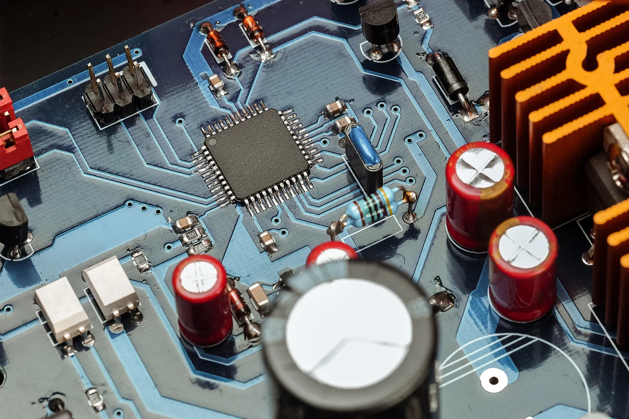
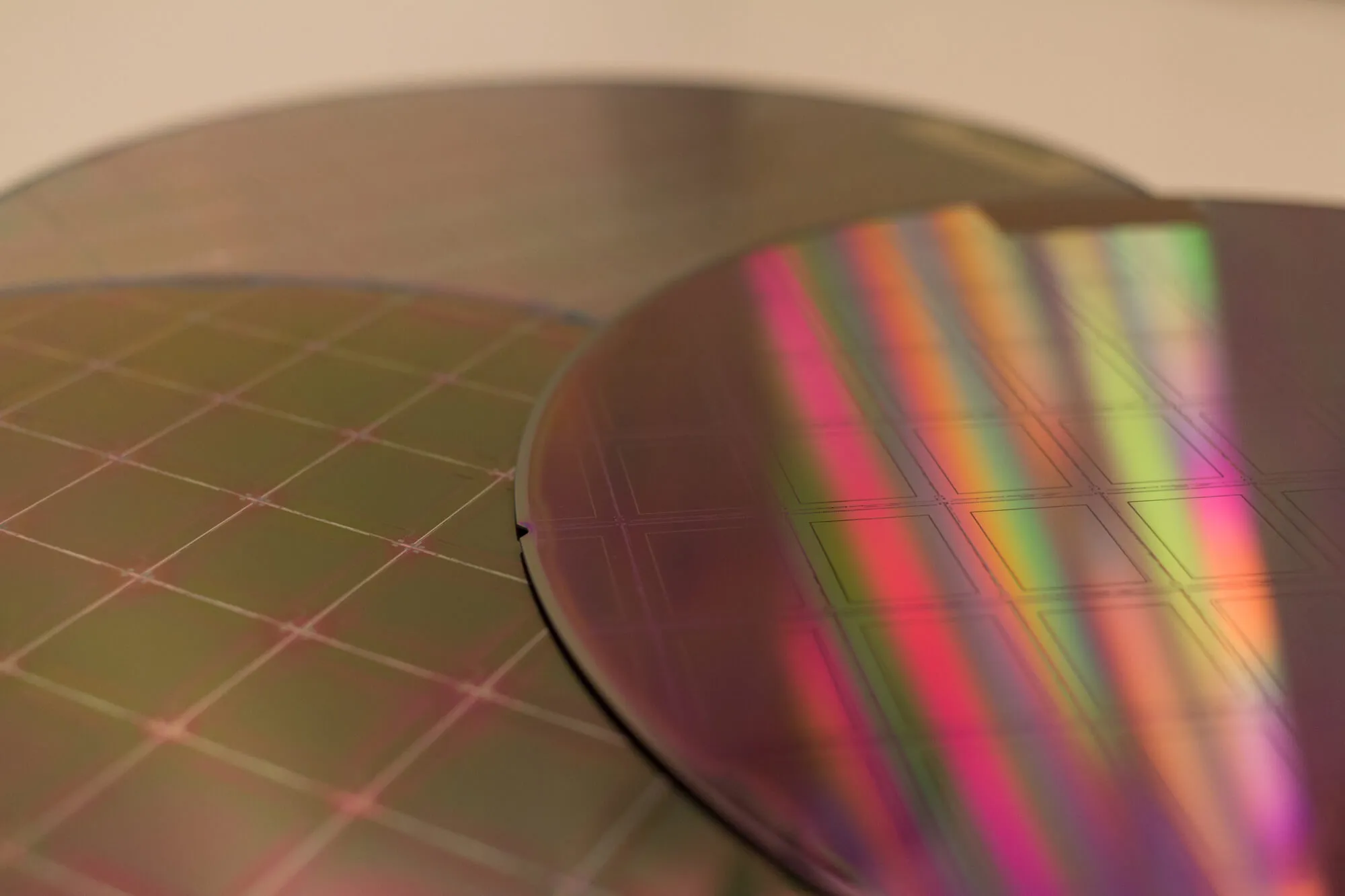
InP wafers, or indium phosphide wafers, are a type of semiconductor material composed of indium (In) and phosphorus (P) atoms. They are the base material for various electronic and optoelectronic devices, particularly in telecommunications, optoelectronics, and photovoltaics. These wafers have several desirable properties that make them suitable for these applications.
They have a direct bandgap, enabling efficient light emission and absorption, making them ideal for optoelectronic devices such as lasers, photodetectors, and photovoltaic cells. Additionally, InP wafers exhibit high electron mobility, allowing faster and more efficient electronic devices. These unique characteristics have increased demand for InP wafers in various industries, including solar energy, quantum computing, and next-generation optoelectronics.
InP-based Multi-junction Solar Cells
InP wafers have shown great potential for use in multi-junction solar cells due to their high efficiency and performance. These solar cells can achieve higher energy conversion rates than traditional silicon-based solar cells, making them an attractive option for future solar energy applications. By integrating InP-based solar cells with existing solar technologies, it may be possible to increase the overall efficiency of solar power systems significantly.
Challenges and Opportunities in InP-based Solar Energy Applications
Material availability and cost: InP wafers' limited availability and high cost can challenge their widespread adoption in the solar energy industry. However, ongoing research and development efforts may lead to more cost-effective production methods, making InP-based solar cells more accessible.
Manufacturing scalability: To meet the growing demand for solar energy solutions, scalable manufacturing processes for InP-based solar cells must be developed. This could involve the optimization of existing techniques or the development of new methods tailored to InP wafers.
Environmental impact and sustainability: The environmental impact of InP wafer production should be considered when assessing its potential for use in solar energy applications. Sustainable manufacturing practices and the responsible management of resources can help minimize this impact.
InP Wafers as a Platform for Quantum Computing Devices
The unique properties of InP wafers, such as low noise and high electron mobility, make them an ideal platform for quantum computing devices. InP-based qubits can enable the development of high-speed, energy-efficient quantum processors and facilitate integration with other quantum technologies.
Potential breakthroughs in quantum computing enabled by InP wafers:
High-speed, energy-efficient quantum processors: InP-based quantum processors can outperform traditional silicon-based processors, offering significant speed and energy efficiency improvements.
Quantum communication networks: InP wafers can potentially enable the development of quantum communication networks, facilitating secure, high-speed data transfer between quantum devices.
Enhanced quantum error correction: The properties of InP wafers can help improve quantum error correction techniques, increasing the reliability and stability of quantum computing systems.
InP Wafers in Advanced Photonic Integrated Circuits
InP wafers have the potential to enable the development of compact, energy-efficient, and high-speed photonic integrated circuits for use in next-generation optoelectronic devices. By integrating InP-based components with existing optoelectronic technologies, it may be possible to create advanced devices with superior performance and functionality.
InP-based Terahertz (THz) Devices
This material can potentially be used to develop terahertz (THz) devices with imaging, sensing, and communications applications. Challenges in THz device fabrication, such as material growth and processing, must be addressed to realize the full potential of InP-based THz devices.
Emerging Industries and Applications
InP Wafers in Biomedical Devices
Biosensors and lab-on-a-chip technologies: InP wafers can potentially be used to develop advanced biosensors and lab-on-a-chip technologies, enabling more accurate and efficient detection and analysis of biological samples.
Advanced imaging systems: InP-based imaging systems can offer improved resolution, sensitivity, and speed compared to traditional imaging technologies, making them attractive for biomedical applications.
Advanced driver-assistance systems (ADAS): InP-based sensors and optoelectronic components can enhance the performance of ADAS, leading to improved safety and efficiency in the automotive industry.
Vehicle-to-everything (V2X) communication systems: InP wafers can potentially enable the development of high-speed, energy-efficient V2X communication systems, facilitating seamless communication between vehicles and other connected infrastructures.
Challenges and Opportunities for InP Wafer Applications
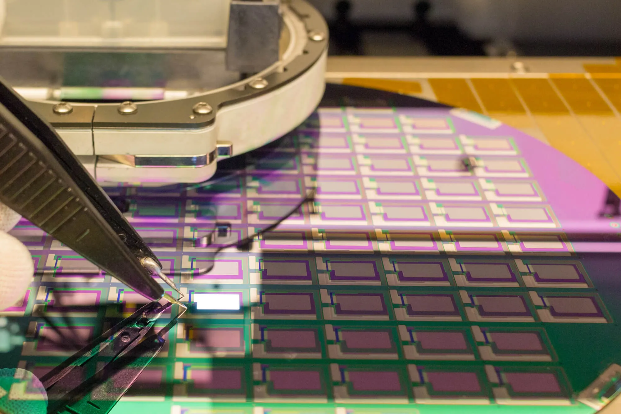
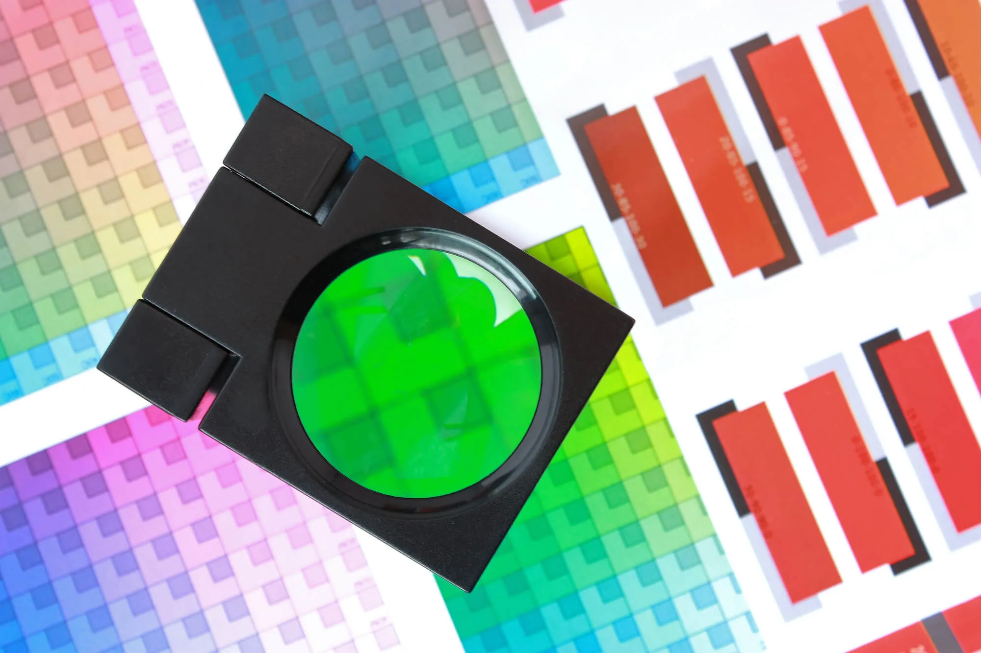
Material synthesis and processing techniques: To fully unlock the potential of InP wafers, improvements in material synthesis and processing techniques are required. This includes refining existing methods and exploring innovative approaches to produce high-quality InP wafers.
Device fabrication and integration: Developing fabrication methods that can efficiently and reliably produce InP-based devices is crucial to realizing the full potential of InP wafers in various applications. Additionally, seamless integration of InP devices with other technologies is essential for creating advanced systems.
Market Trends and Growth Projections
Key players and competitive landscape: Understanding the key players in the InP wafer market, their strategies, and the competitive landscape is crucial for predicting future trends and potential growth opportunities.
Potential for market expansion and diversification: As silicon wafers find new applications in emerging industries, there is a significant market expansion and diversification potential. This presents opportunities for established players and entrants in the InP wafer market.
Societal and Environmental Implications
Energy efficiency and sustainability: The adoption of InP wafers in various applications can lead to increased energy efficiency and reduced environmental impact, contributing to global sustainability goals.
Ethical considerations and potential unintended consequences: As InP wafers are integrated into new applications, it is essential to consider these technologies' ethical implications and potential unintended consequences. This includes addressing data privacy, security, and the potential impact on employment and social equity.
As research and development efforts continue, InP wafers will likely be crucial in driving technological advancements across various sectors. Addressing the challenges and opportunities associated with InP wafer applications will be essential for unlocking their full potential and ensuring a sustainable and prosperous future.
Are You Interested in Getting InP Wafers?
Here at Wafer World, our team can provide you with high-quality InP wafers that can cater to your industry. Contact us today to learn more about the products we offer.