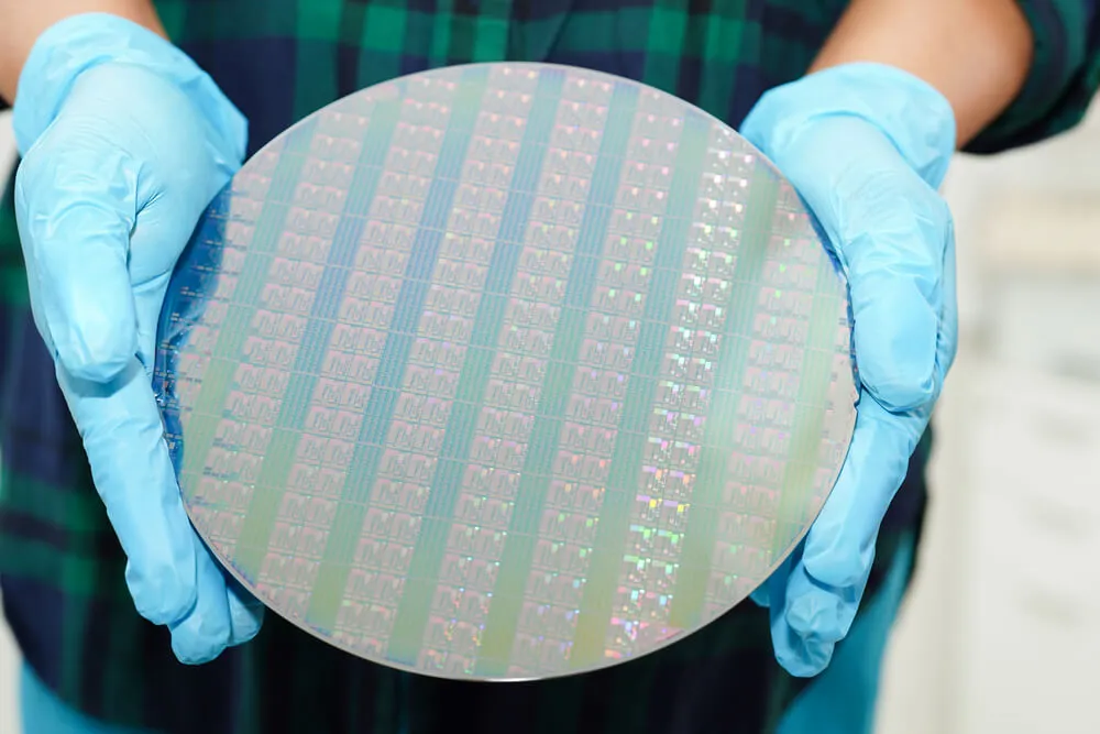
Doping plays a pivotal role in shaping the electrical properties of semiconductor materials like GaAs (Gallium Arsenide) wafers, influencing their functionality in various electronic devices. GaAs wafers can be doped with different types of impurities to achieve specific electrical characteristics, with two primary types being N-type and P-type doping.
N-type doping involves introducing impurities into the GaAs crystal lattice that have an excess of electrons compared to the host material. Common dopants for N-type doping in GaAs wafers include silicon (Si) or tellurium (Te). These dopants have five valence electrons, with the extra electron becoming a conduction electron when incorporated into the GaAs lattice.
As a result, N-type doped GaAs wafers exhibit an abundance of free electrons, enhancing their conductivity. This makes N-type GaAs wafers suitable for applications requiring high electron mobility, such as in high-frequency RF devices and photovoltaic cells.
P-type doping involves introducing impurities that create electron deficiencies or "holes" within the GaAs crystal lattice. Common dopants for P-type doping in GaAs wafers include zinc (Zn) or beryllium (Be), which have only three valence electrons. When these dopants substitute gallium atoms in the GaAs lattice, they create "holes" that act as mobile charge carriers. Consequently, P-type doped GaAs wafers exhibit enhanced hole conductivity. P-type GaAs wafers find applications in devices such as light-emitting diodes (LEDs), laser diodes, and power amplifiers.
N-type doping results in an excess of electrons, increasing conductivity, while P-type doping creates "holes," enhancing hole conductivity.
N-type GaAs wafers are suitable for applications requiring high electron mobility, whereas P-type GaAs wafers are preferred for devices relying on hole conduction.
The choice between N-type and P-type doping depends on the specific requirements of the device being fabricated, such as desired carrier concentration, conductivity, and performance characteristics.
Understanding the role of doping in GaAs wafers from Wafer Word, specifically N-type and P-type doping, is crucial for tailoring their electrical properties to meet the diverse needs of semiconductor devices across various industries. Call us today to order!


