.webp)
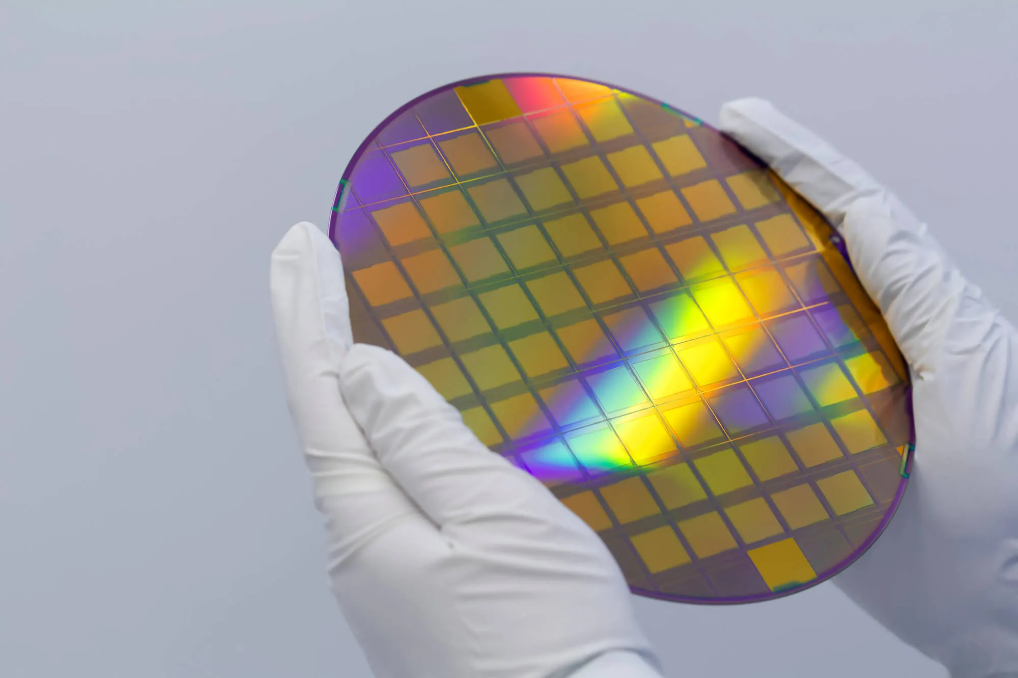
While GaAs or Gallium Arsenide is an excellent component when utilizing it in integrated circuits and field-effect transistors, it also has its issues when it comes to manufacturing and processing them. This can be attributed to the fact that the fabrication processes of GaAs are large and complicated. If you’re interested in learning more about GaAs reclaim wafers, here are some usual problems it often faces.
.webp)
The price of a single-crystal GaAs substrate, which has prevented mass production of GaAs, is one major disadvantage of this material. Additionally, similar to silicon devices, processing steps frequently sow the seeds of GaAs contact reliability issues. These processing steps also help to lower contact quality and create conducting projections that pose a threat to short the newly created GaAs layer.
Ion implantation has not developed quickly as a method for fabricating GaAs devices. The reason for this delay is that integrated circuit technologies using GaAs have recently expanded due to the later maturation of implantation doping processes in GaAs.
The reproducibility and homogeneity of doping, whose implantation in silicon has been established, is necessary for these integrated circuit technologies. The most noticeable feature of implantation in GaAs that sets it apart from silicon is the dissociation of GaAs caused by the loss of arsenic.
The existence of crystal defects (dislocations, precipitates, point defects, etc.), either inherent or created during technical processing, affects the performance and dependability of GaAs devices. The Cottrell atmospheres, often introduced by dislocation and the interaction of the crystal matrix with the crystal, increase the micrometric inhomogeneity of the crystal.
GaAs have low thermal conductivity (about one-third that of Si), which causes heat to be generated primarily in a few isolated areas with high thermal gradients and non-isothermal surfaces. For two main reasons, it is essential to have a thorough understanding of heat generation and temperature prediction at sub-micron length scales to characterize the thermal behavior of GaAs devices properly.
At Wafer World, we don’t only provide high-quality wafers; we also provide helpful information for our clients. Give us a call today to get a quote!


