Silicon wafers are relatively anonymous components of almost all modern electronics. They allow our phones to retain their small size without sacrificing any of their efficiency, they help transfer radio waves and even play an integral part in many solar cell systems. Needless to say, that despite their relative anonymity, silicon wafer manufacturers play a pivotal role in the present and the future of our technology. As industry leaders in silicon wafer technology, Wafer World wants to take this opportunity to educate you on the basics of silicon wafers and help you understand just how important these largely unknown components actually are. https://youtu.be/Y_5NePTRlSI
Silicon wafers are everywhere, yet few of us are even aware of the role they play in our everyday lives. These wafers function as semiconductors that facilitate the transfer of radio and electromagnetic waves and are thus used when fabricating integrated circuits in many electronic devices.
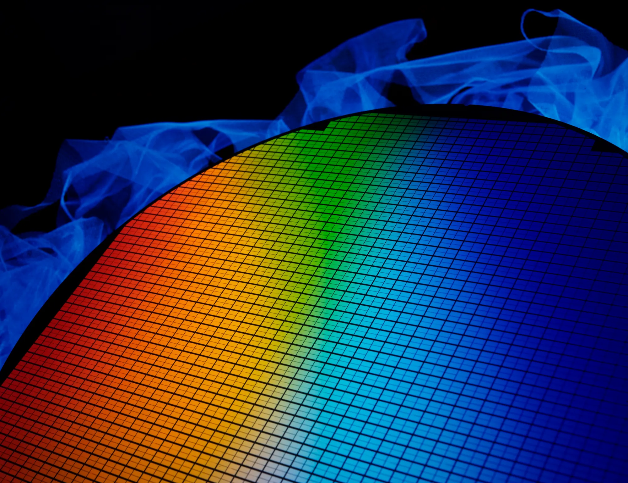
There are many reasons why silicon is one of the most commonly used materials by silicon wafer manufacturers. For starters silicon is one of the most abundant elements in our planet, making up as much as 27.7% of the Earth’s crust. Silicon has a crystalized, diamond-like body that makes it especially effective in conducting electromagnetic waves. The element also has a high number of free electrons, which help conduct high levels of electricity. Silicon is also very malleable, making it a perfect material for creating hyper thin and flat wafers. Although other materials are more effective semiconductors, the combination of abundance, physical properties, and conductivity, make silicon the preferred material for many silicon wafer manufacturers.

A semiconductor is any material that has a level of conductivity somewhere between conductors and nonconductors. The post popular semiconductors include silicon, germanium, and gallium arsenide. Historically, electronics were made with vacuum tube technology, but thanks to the innovation of semiconductors, electronic devices can now be made smaller, faster, and more reliable.
Silicon wafer manufacturers can break down their process into three main steps; growing, slicing, and cleaning.
The first step in the silicon wafer manufacturing process is growing a silicon ingot. This is done using the Czochralski method which requires that poly-crystalline silicon (which is essentially high purity silicon) is melted at a temperature of 1400 degrees Celsius. Once the material reaches the melting point, a seed crystal is mounted on a rod and then dipped into the molten silicon.
Once the seed crystal is removed is the next step for silicon wafer manufacturers is slicing the material. After the silicon ingot is fully grown, the material is cut down to shape slightly larger than the intended use. Then a diamond edge saw is used to carefully slice the silicon wafers.
This is perhaps the most important step in the manufacturing process as the conductivity of the wafer is largely determined by its lack of imperfections. The cleaning process takes place in a ‘clean room’ in which workers wear specialized gear that prevents them from unintentionally depositing foreign particles onto the silicon wafer.

Throughout the manufacturing process, silicon wafers undergo a doping procedure. Doping is the process of adding a substance called a ‘dopant’ which serves the role of increasing the base conductivity of the element. The most common dopant agents are Boron (p-type) and phosphorous, arsenic, and antimony (n-type).
The reason that the Czochralski method of silicon seeding is used in the first place is that semiconductors require a high level of purity to work efficiently. The waves carried to through the material are minuscule and highly sensitive to even the smallest alterations. For this reason, silicon wafer manufacturers take great care in maintaining as close to 100% purity in the product as possible. https://youtu.be/6OyCL8J_RGU
Silicon wafer manufacturers use two different grades of silicon substrates: standard silicon and ultra-flat silicon wafers.
Standard silicon wafers have similar properties to glass and thus are most commonly used for biological applications. Due to their thickness and composition, this grade of a silicon wafer is used in thin-film research, sample substrates, and micro-fabrications. They also make excellent surfaces for SEM imaging as they offer almost no background interference.
Ultra-flat wafers have a much higher standard and specification than standard silicon wafers. These have much more common use in micro-fabrication because they can withstand high demand applications. Ultra-flat silicon wafers can also serve the same biological purposes as standard wafers as they too offer a glass-like structure and minimal background interference.
Silicon wafers are the understated hero of modern technology. These nifty little slides help keep all sorts of technical equipment performing at their full capacity. You can find silicon wafers in:
The applications of silicon wafers are nearly limitless and as you can see, silicon wafer manufacturers have influenced many aspects of the world around you without you even knowing it.

Silicon wafer manufacturers put the wafers through many tests before they are ready to submit the product to the market. These tests simulate the stresses and long-term wear and tear on the wafers. Even with these tests, silicon wafers can still be damaged. Some of the common causes of damage include:
There are three key vectors used to determine the quality and purity of a silicon wafer: light point defects, TVV, and warping.
Also referred to as LPDs, these are unwanted particles found on the surface of a wafer that interferes with conductivity.
TVV helps determine the difference between the thickness between the thickest and thinnest part of the wafer. The lower the difference, the more effective the wafer.
Warp in a wafer can greatly hinder its conductivity. Silicon wafer manufacturers use a measurement known as GTIR to determine the maximum peak to valley deviation.

Silicon wafers are an integral component of the technology we utilize in our everyday life. Choosing the right manufacturer could mean the difference between a successful product and one riddled with inefficiencies. For the best in silicon wafer manufacturers, contact us today!


