.webp)
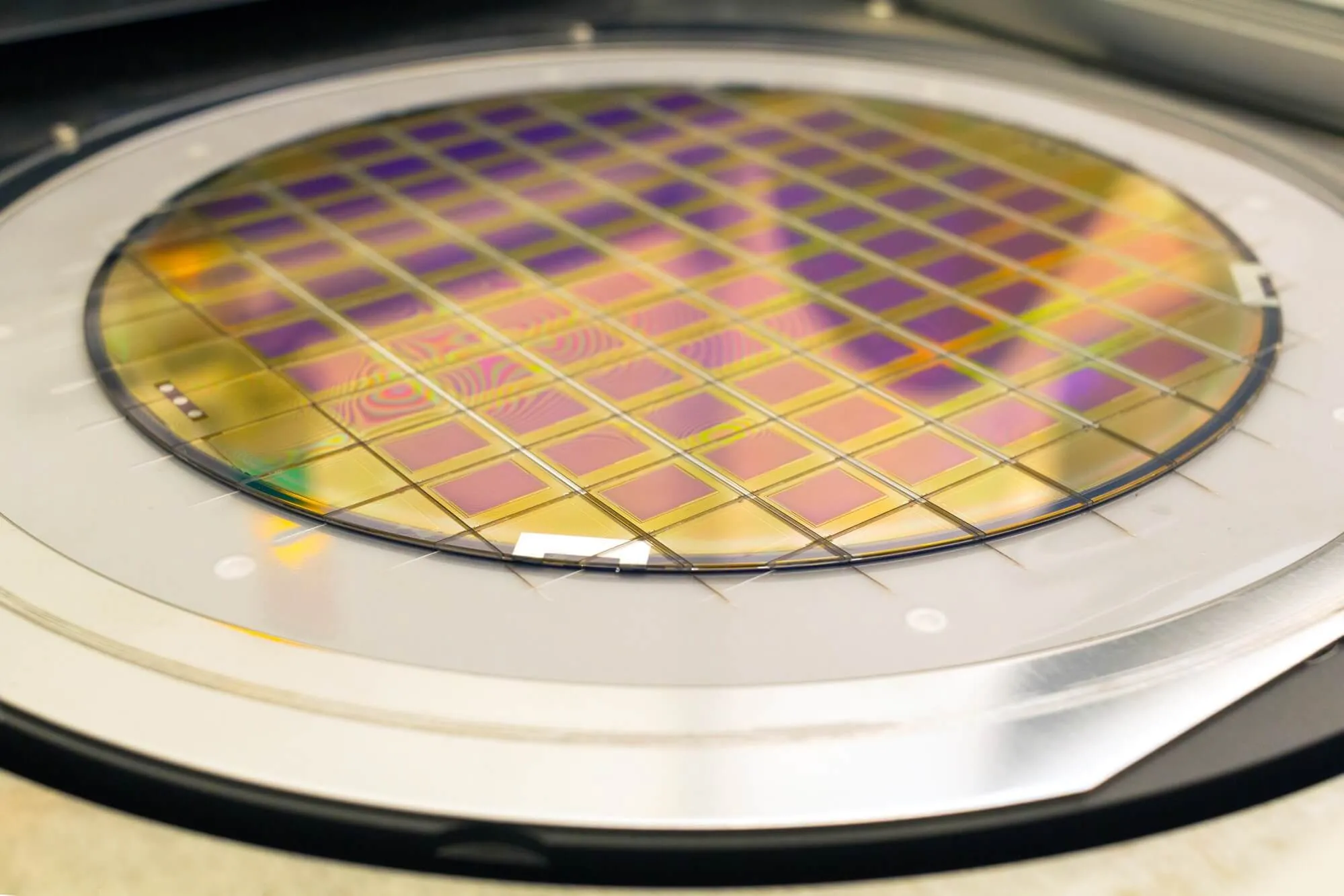
In the fast-evolving landscape of scientific discovery, float zone wafers quietly take the spotlight, serving as crucial catalysts for progress and pushing the boundaries of technology and science. With their distinctive characteristics and unmatched purity levels, these wafers play a hidden yet pivotal role in many cutting-edge research projects.
In this exploration, we unveil the unconventional uses of float zone wafers, shedding light on their indispensable contributions to advancing our understanding and capabilities.
Float zone wafers are silently influencing the field of quantum information processing, a domain poised to transform computing as we know it. Researchers harness the exceptional purity of float zone wafers to craft qubits—the fundamental elements of quantum computers.
The uniformity of the crystal lattice allows for meticulous manipulation of quantum states, propelling us into a future where quantum computers tackle intricate problems at speeds beyond the reach of classical counterparts.
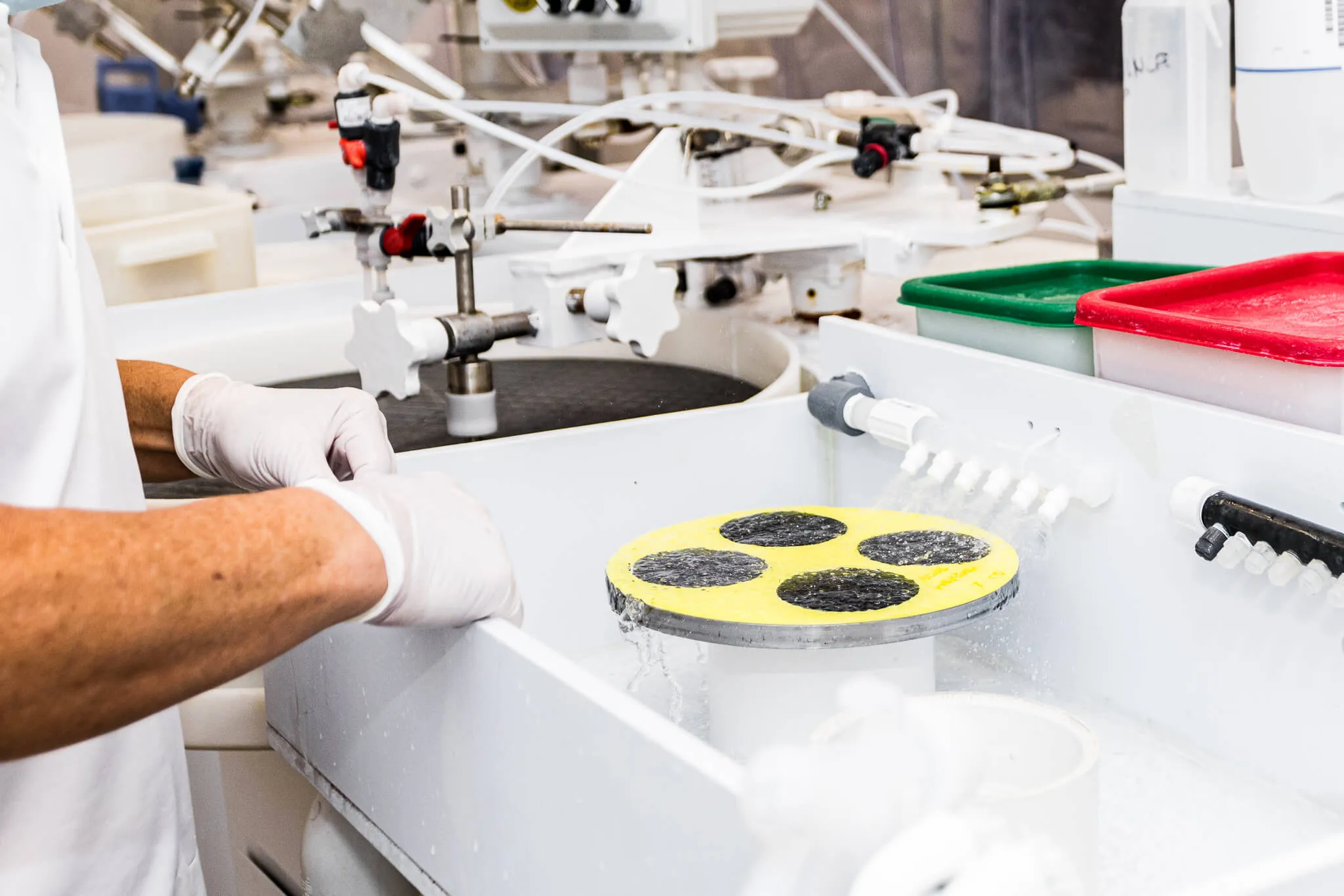
Float zone wafers emerge as unsung heroes in pursuit of smaller, faster, and more energy-efficient electronics. Researchers employ these wafers to fabricate advanced semiconductor devices, boasting enhanced performance characteristics. The crystal purity minimizes defects, resulting in semiconductor components with superior electrical properties.
From high-frequency transistors to ultra-sensitive sensors, float zone wafers quietly shape the trajectory of next-generation electronic devices.
In the realm of optoelectronics and photonics, float zone wafers provide the canvas for developing cutting-edge light-emitting and detecting devices. Controlled crystal growth allows researchers to engineer materials with specific optical properties. This capability is instrumental in creating efficient light-emitting diodes (LEDs), lasers, and photodetectors for telecommunications and biomedical imaging applications.
Float zone wafers are foundational elements for crafting novel materials and structures in materials science and nanotechnology. Researchers leverage the exceptional purity and uniformity of these wafers to cultivate thin films and nanoscale structures with atomic precision. This level of control opens avenues for developing advanced materials with tailored electronic, magnetic, and optical properties, advancing nanoelectronics, spintronics, and other cutting-edge technologies.
Float zone wafers are making strides in renewable energy technologies, particularly photovoltaics. Researchers utilize the high purity and crystal uniformity of float zone wafers to enhance solar cell efficiency. The precise control over crystal growth enables the production of silicon wafers with minimal defects, contributing to the development of sustainable and efficient solar energy solutions.
Float zone wafers are indispensable in quantum sensing, where manipulating individual quantum states leads to ultra-sensitive measurements. High-purity crystals facilitate the creation of sensors capable of detecting minute changes in physical quantities like magnetic fields or gravitational forces.
The precision in fabricating quantum sensors using float zone wafers unlocks possibilities in fundamental research and applications, from studying exotic quantum phenomena to developing advanced medical imaging technologies.
In biomedical research, float zone wafers contribute to developing advanced medical devices and diagnostic tools. Researchers leverage the precision and purity of float zone wafers to manufacture microelectromechanical systems (MEMS) and bioelectronic devices, paving the way for innovations such as implantable sensors, drug delivery systems, and lab-on-a-chip technologies.
Float zone wafers extend their applications beyond Earth, contributing to advancing space exploration technologies. The reliability and performance of semiconductor devices manufactured using float zone wafers make them ideal for space missions, from satellite systems to interplanetary probes.
Float zone wafers play a role in achieving superconductivity at higher temperatures, contributing to the fabrication of advanced superconducting materials. This innovation opens avenues for developing superconducting devices, such as high-performance magnetometers and quantum levitation systems.
Float zone wafers are integral to environmental monitoring, where high-precision sensors are crucial for detecting and analyzing pollutants and environmental changes. Researchers leverage the purity and uniformity of float zone wafers to develop sensors with enhanced sensitivity and accuracy.
Float zone wafers take the lead in terahertz technology, exploring the use of electromagnetic waves in the terahertz frequency range. Researchers use float zone wafers to fabricate terahertz emitters, detectors, and modulators with unparalleled precision, offering solutions for medical diagnostics, security screening, and material characterization.
Float zone wafers are making notable strides in acoustic devices, utilizing sound for sensing and communication applications. Researchers harness the distinctive properties of float zone wafers to fabricate high-frequency acoustic wave devices. These devices are applied in wireless communication, sensing technologies, and medical imaging.
The precision provided by float zone wafers plays a crucial role in crafting compact and effective acoustic wave devices with a variety of functionalities.
Float zone wafers are significantly advancing augmented reality (AR) optics, shaping immersive experiences across diverse industries. Researchers exploit the purity and precision of float zone wafers to create high-quality optical components for AR devices. This advancement improves display clarity, color accuracy, and the overall user experience in augmented reality applications, spanning from gaming and education to healthcare and industrial training.
In the continually evolving realm of electronics, float zone wafers are challenging conventional design norms by contributing to the evolution of flexible electronics. The outstanding uniformity of crystal structures enables the development of flexible and stretchable electronic components. This innovation is paving the way for flexible displays, wearable electronics, and conformal sensors.
Float zone wafers are subtly reshaping the electronics landscape, allowing technology to seamlessly integrate into our daily lives.
In the intricate tapestry of scientific exploration, float zone wafers weave threads of untold possibilities. From the quantum realm to outer space and from biomedical applications to environmental monitoring, these wafers are indispensable for researchers pushing the boundaries of technology and science.
As we unravel the unique properties and applications of float zone wafers, we gain a deeper understanding of the materials themselves and a glimpse into the transformative impact they have on the forefront of research.
The path of invention using float zone wafers from Wafer World develops as a series of possibilities, balancing technological advancement with the never-ending pursuit of knowledge. Contact us to order!


