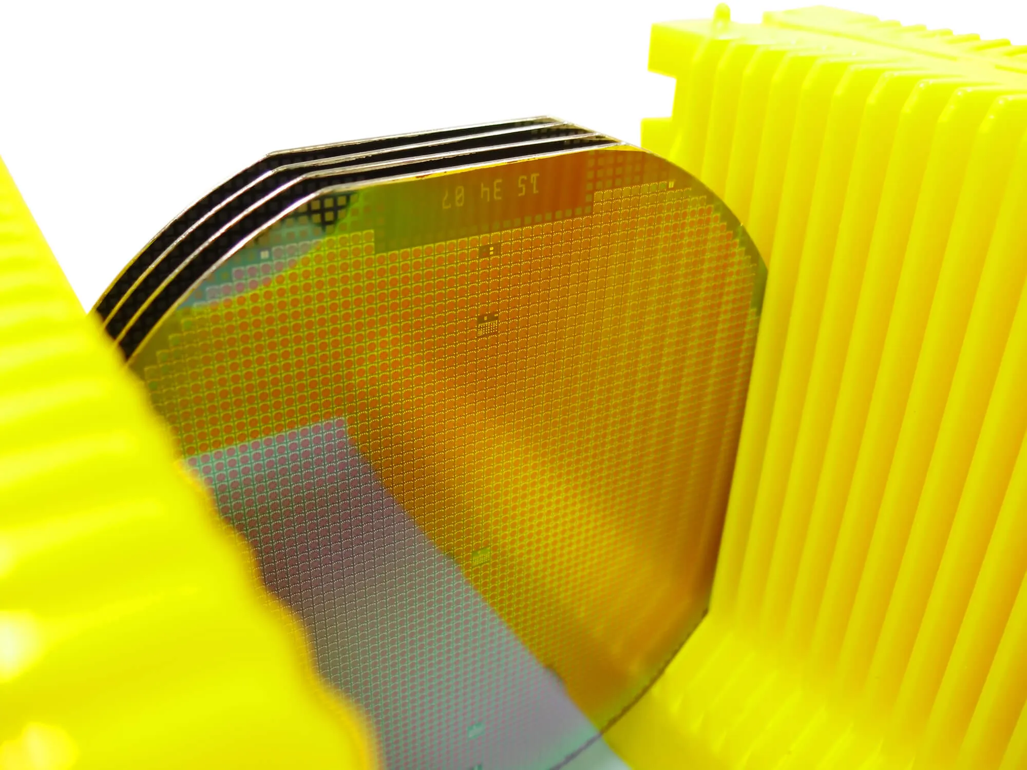
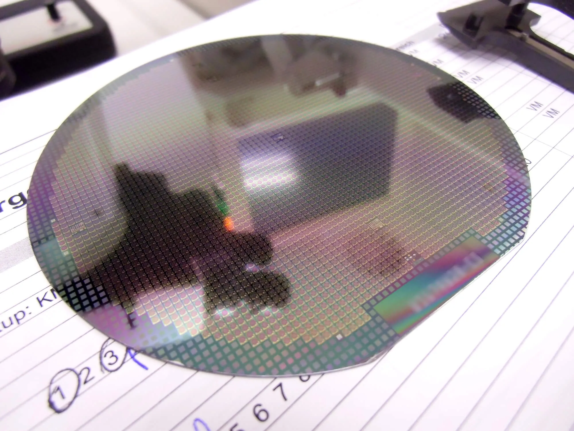
The typical wafer thinning procedure combines mechanical grinding with stress relief from polishing or etching. The production and handling of these ultra-thin wafers differ significantly from conventional wafers because of the unique mechanical characteristics of these thin-film semiconductors. This article will review the developments in ultra flat wafer technology, from the manufacturing process to wafer transportation and device application.
.webp)
Die thickness is one of several essential factors in creating ultra-thin wafers. However, the wafer diameter is rising while the chip thickness is decreasing, and thicker silicon is needed to manufacture wafers with greater wafer diameters. Thinning techniques are becoming more and more crucial since processing demands that wafers be thinner and thinner die are more appealing.
The best method for creating ultra-thin wafers is to thin the entire wafer at the back end, i.e., after finishing the front-side device processing. As a result, new or enhanced thinning techniques are created. Manufacturers use quick and inexpensive methods. To reach the final wafer thickness of 20m, the thickness tolerance should be adjusted to 1m.
The wafer needs to be thinned to create ultra-thin dies. Traditionally, wafer thinning has been accomplished by grinding the wafer's reverse side. The surface can be polished by wet etching or dry plasma etching following mechanical grinding, or it can be combined with polishing like in the conventional chemical-mechanical-polishing procedure (CMP).
The dies are subsequently separated into pieces by DRIE etching on a carrier wafer or sawing on a thermal or UV-sensitive dicing tape. Dicing now occurs due to grinding the wafer backside until pre-cut grooves on the front side are reached, thanks to a recent change in the procedure. After that, plasma etching is typically used to complete the ground surface and to relieve the dies of tension.
At Wafer World, our team can provide you with ultra-flat wafers to help you develop existing or new technologies. Give us a call today to learn more about our products.


