Wafer bonding is a vital process in modern chip development, enabling the creation of smaller, faster, and more efficient electronic devices. As silicon wafer suppliers expand and semiconductor technology evolves, traditional two-dimensional chip designs face physical and performance limitations.
Wafer bonding offers a way to overcome these challenges by allowing vertical integration, material combination, and advanced packaging techniques—all essential for producing high-performance chips used in smartphones, AI systems, sensors, and more.
EMBEB:
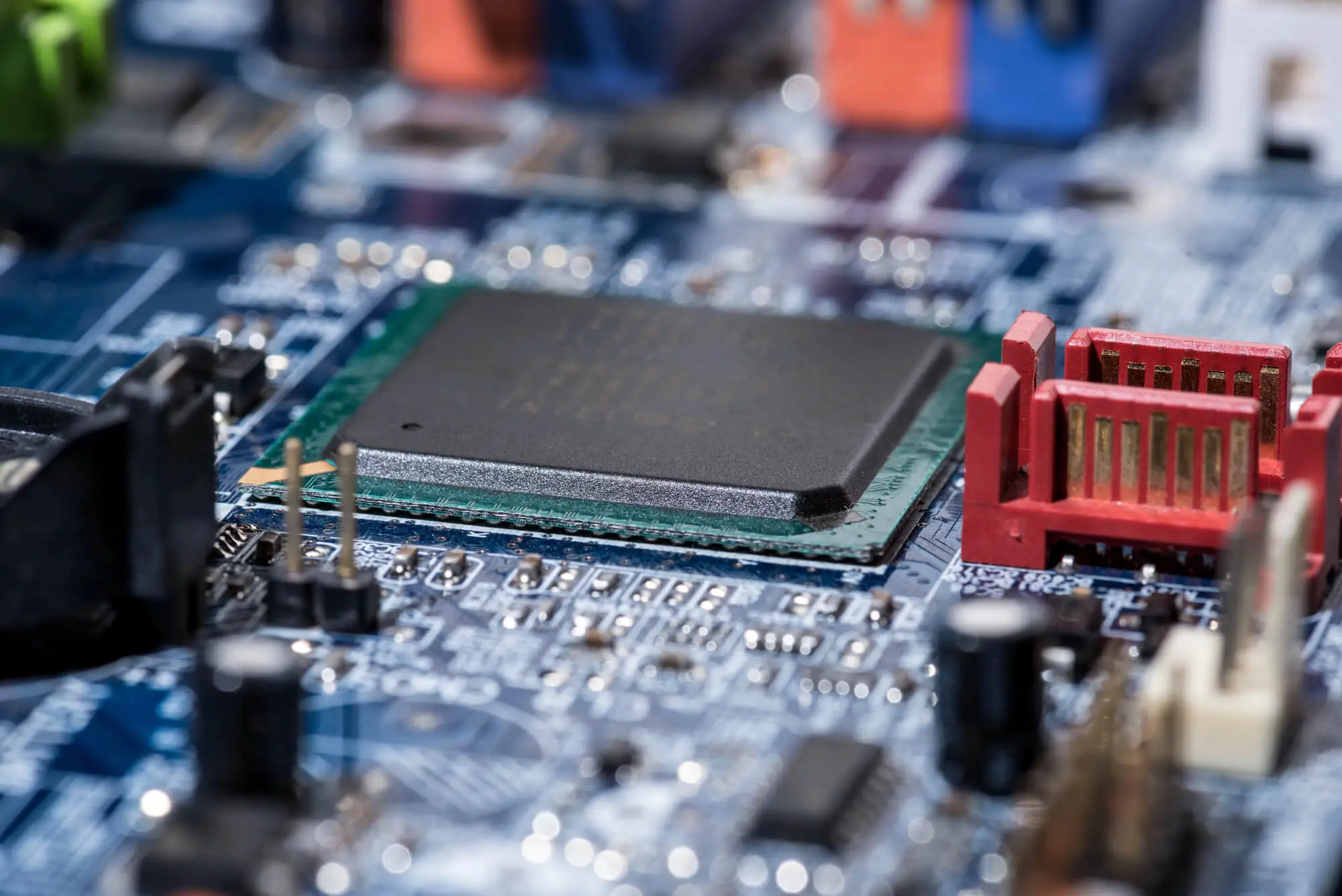
At its core, wafer bonding is the process of joining two semiconductor wafers together to form a single, unified structure. This technique allows multiple layers of circuitry, materials, or functions to be integrated with high precision, which offers several benefits to chip manufacturers, such as:
Several types of wafer bonding techniques exist, each with unique mechanisms, requirements, and advantages. Choosing the right bonding method can impact the final product's performance, reliability, and manufacturing cost.
Direct bonding, also known as fusion bonding, involves joining two ultra-flat, smooth, and clean silicon wafers without any intermediate layer. The bonding occurs at the atomic level through Van der Waals forces, which can transform into covalent bonds with subsequent high-temperature annealing.
It is used in applications such as 3D integrated circuits, SOI (Silicon-On-Insulator) wafers, and MEMS devices. Its benefits include:
Anodic bonding, also known as electrostatic bonding, typically bonds silicon to a glass wafer containing mobile ions (like borosilicate glass). A high voltage and moderate temperature (200–400°C) are applied, causing ions to migrate and form a strong electrostatic attraction between the wafers.
It can be used for manufacturing MEMS sensors, biomedical devices, microfluidic systems, and packaging technologies. Some of its benefits include:
This method uses a polymer adhesive (such as SU-8, BCB, or epoxy) as an intermediate bonding layer between wafers. The adhesive is spin-coated, and the wafers are pressed together and cured using heat or UV light.
Its main applications include BioMEMS, optical devices, flexible electronics, and temporary bonding for wafer handling. It can have several advantages when developing electronics, such as:
Eutectic bonding involves forming a metal-silicon interface (often gold-silicon or aluminum-silicon) at a eutectic point, where the materials melt and bond at a lower temperature than their individual melting points.
It can be used for manufacturing RF MEMS, pressure sensors, power electronics, or optical packaging, because it offers advantages such as:
Thermocompression bonding involves pressing two wafers together under high temperature and pressure, usually with a metal layer (like gold or copper) between them. Unlike eutectic bonding, it doesn’t require melting.
It’s used for developing 3D IC stacking, sensor packaging, and micro-bump interconnects. Its benefits include:
Hybrid bonding combines features of both direct wafer bonding and thermocompression bonding. It includes dielectric-to-dielectric bonding for mechanical strength and metal-to-metal bonding for electrical connectivity, often used in advanced 3D IC packaging.
Applications include 3D NAND, logic-memory stacking, high-end processors, and AI chips. This bonding technique offers benefits such as:
Silicon wafer bonding is a versatile and essential technology in semiconductor manufacturing. From the simplicity of adhesive bonding to the precision of direct and hybrid bonding, each technique offers unique benefits suited to specific applications.
As devices continue to shrink and demand higher performance, advanced bonding methods like hybrid and thermocompression bonding are becoming more prominent—particularly in AI, 5G, and 3D integration. Here at Wafer World, we strive for the continued development and optimization of wafer technologies.
Contact us today and learn more about our substrates—and how to make the most out of them.


