When a spec sheet lists a wafer’s flatness tolerance, it’s easy to read it as one more number in a long list. But in processes like photolithography, where patterns are printed at nanometer scales across the entire surface, a few microns of variation can be the difference between a usable wafer and a costly reject.
That’s why ultra flat wafers exist: silicon and compound semiconductor wafers manufactured to unusually tight flatness tolerances, with minimal variation in thickness from edge to edge.
Still, “ultra flat” doesn’t mean much on its own. Flatness is measured in several different ways, and each one tells you something different about how a wafer will perform.
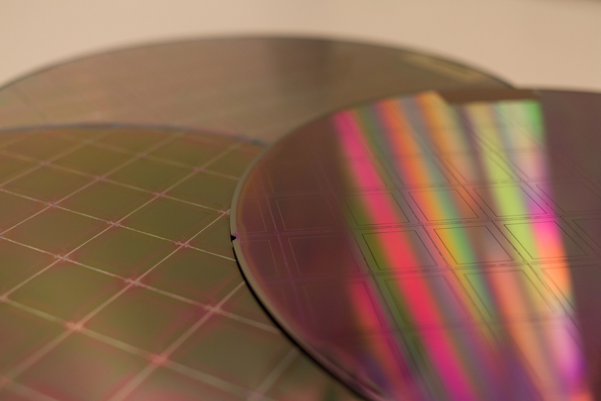
Flatness describes how much a wafer's surface deviates from a perfectly flat reference plane, and it is measured separately from thickness itself. A wafer can meet its target thickness on average while still containing localized high and low spots that affect how it behaves under processing equipment.
Ultra flat wafers minimize that variation across the usable surface, which matters most in processes that depend on precise, repeatable contact or alignment.
Ultra flat wafers are often thin as well, and thinner wafers are more fragile during handling and processing. Carrier wafers and specialized handling equipment are commonly used to support the wafer through grinding, etching, and inspection steps, reducing the risk of warping or breakage before the wafer reaches its final application.
That handling step is worth planning for early, since retrofitting a process around a fragile substrate after the fact tends to be more disruptive than designing for it from the start.
No. While research and MEMS development are common use cases, ultra flat wafers also support commercial applications like flexible electronics, sensors, and photovoltaics.
Not automatically. Thickness and flatness are related but distinct measurements, and a thin wafer can still have flatness variation if processing controls are not tight enough.

Matching flatness tolerance to your actual process requirements avoids both underperformance and unnecessary cost. Wafer World can help you review specifications for ultra flat wafers across silicon and other materials. Request a quote and our team can help match the tolerance to your project.