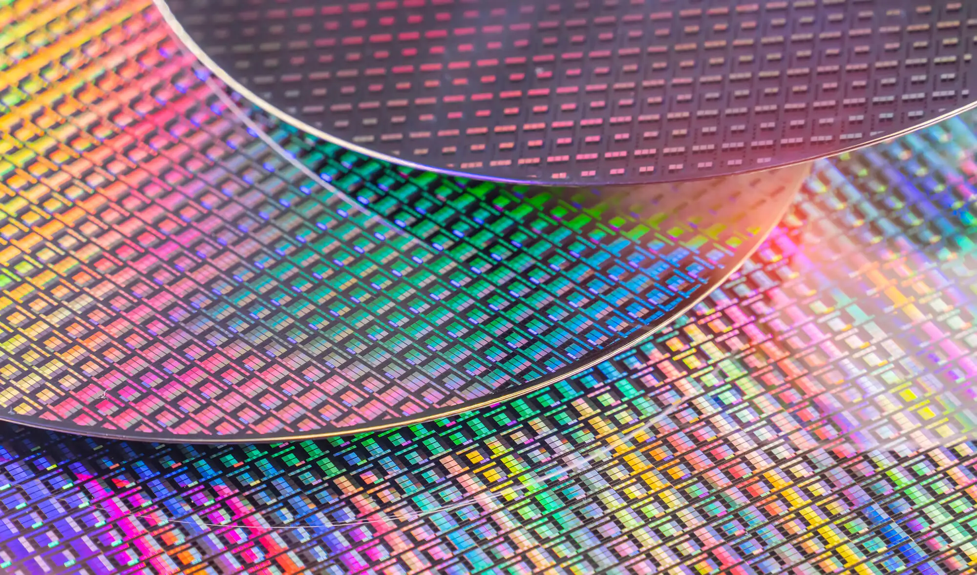
As semiconductor devices continue to shrink and become more powerful, the demand for ultra-thin wafers in advanced packaging, MEMS, and 3D integration has surged. However, handling and processing these fragile substrates is no easy feat. That’s where carrier and handle wafers come in.
These supporting substrates provide the mechanical strength and thermal stability necessary to safely process thin wafers through back-end and front-end processes, such as grinding, etching, deposition, or lithography. But not all carrier wafers are the same—and choosing the right one is crucial for process success.
Carrier wafers, also known as handle wafers, are temporary support substrates used to hold ultra-thin device wafers during semiconductor manufacturing. Once the device wafer has been thinned (down to 50 μm or even less), it becomes too fragile to undergo further processing independently. A carrier wafer provides the needed mechanical support throughout the rest of the process flow.
After processing, the carrier is removed through a debonding process, allowing the thin wafer to continue to dicing, testing, or packaging. So, carrier wafers are not part of the final product—they’re part of a temporary bonding and debonding process that protects the thin wafer while ensuring precision and yield.
Carrier wafers are available in various materials, each offering distinct properties in terms of thermal stability, optical transparency, chemical resistance, and mechanical strength.
Some common carrier wafer materials include:
Thin wafers are essential in applications like:
Ultra-thin wafers are highly vulnerable to breakage during handling, wafer warpage under thermal stress, or particle contamination. Carrier wafers prevent these issues by stabilizing the wafer during grinding, CMP, lithography, etching, and other processes, enabling high throughput with low breakage rates.
They also allow compatibility with standard wafer tools (like CMP or DRIE systems).
One of the most critical factors in selecting a carrier wafer is how it will be released from the device wafer. Different applications require different debonding methods, which in turn influence the choice of carrier material and the process flow.
The most common debonding approaches include:
Chemical release carriers are separated from device wafers using a solvent or chemical agent that dissolves the temporary adhesive layer. This option is selected because it’s gentle on sensitive devices and compatible with many materials. The disadvantage, however, is that it requires solvent management and rinse processes.
For that reason, it’s often a go-to method for MEMS, image sensors, or fragile structures that can’t tolerate high heat or stress.
Thermal release carriers use temperature-sensitive adhesives that lose adhesion when exposed to heat (usually 150–200°C). It’s simple and fast, with no chemical residue. However, it requires careful management of the thermal budget.
This method is best suited for applications where solvents are not permitted or where speed is crucial.
Laser debonding involves transparent carrier wafers (like glass) that allow a laser to pass through and break the adhesive bond at the interface. This allows for very fast, localized debonding and minimal wafer stress. The downside is that it requires transparent carriers and precision alignment.
It’s utilized for high-volume production or ultra-thin wafers (<50 µm) where damage must be minimized.
In some cases, physical peeling or separation can be used to remove the carrier, often in combination with low-adhesion adhesives or mechanical fixtures. While this avoids the need for chemicals or heat, there’s a risk of damage if not well-controlled.
For that reason, this method is best for low-cost or low-risk development environments.
The right carrier wafer solution depends on more than just size—it must align with your process, tools, and device sensitivity. Some key factors to consider include:
While selecting the right carrier system is crucial to prevent damaging your ultra-thin substrate, choosing the right provider also plays a fundamental role. A reliable wafer manufacturer ensures consistent wafer thickness, minimal warpage, tight TTV control, and clean surface quality—all essential for high-yield, thin-wafer processing.
Poor-quality wafers can lead to breakage, tool downtime, or process failure, even with a carrier system.
Whether you're working in advanced packaging, MEMS, or photonics, partnering with a trusted wafer supplier helps you maintain process integrity, reduce waste, and accelerate time to market with confidence.
Carrier and handle wafers are critical enablers of thin-wafer processing, supporting the push toward smaller, faster, and more efficient semiconductor devices. But choosing the right carrier isn’t just about picking the right material—it's about aligning the release method, tool compatibility, and process needs to your specific application.
Whether you’re developing MEMS, high-frequency RF devices, or advanced logic ICs, the right carrier system helps reduce breakage, improve yield, and maintain process integrity at scale. Additionally, finding the right ultra-thin wafer provider plays a big role.
At Wafer World, our products undergo stringent quality control methods to ensure our ultra-thin wafers meet all your project’s needs. Contact us today to learn more about our manufacturing process!


