Wafer semiconductors are everywhere around us, from the biggest solar panels to the smallest components of microfabrication equipment. Since the uses for semiconductor wafers are so diverse, the manufacturing process varies depending on the application. Among the many types of wafers, ultra flat wafers are built with the highest specifications. As your leading source for all thing's semiconductor wafers, Wafer World is excited for this deep dive into ultra flat wafers.
Ultra flat wafers are substrates, a thin slice of semiconductor material, made with higher specifications than traditional standard wafers. The high manufacturing requirements are a result of the applications for these wafers. While they can be used in many of the same ways standard wafers are, they are specially made to withstand particularly demanding applications such as being a component in microfabrication equipment. Other common uses for ultra flat wafers are as substrates in biological applications like thin-film research. Their attributes also make these wafers preferred in scanning electron microscopes (SEMs) which are used to scan surfaces and create high-resolution topographic images.
Because ultra flat wafers are, well, ultra flat, it would be impractical to use common measurements like inches. Instead, these wafers are measured in microns, a unit of measure that equals one-millionth of a meter or 1/26,000th of an inch. In American standard measurement, microns are also known as micrometer and carries the abbreviation of ‘μm’.
While standard wafers are usually around 750 microns thick, for a substrate to be considered an ultra-thin wafer, it needs to be under 200 microns in thickness.
Ultra flat wafers tend to be made from the same substances used for standard wafers, the three most common are:
Silicon is by far the most common material used in semiconductor manufacturing. The reason for this element’s popularity is how abundant it is and the low-cost of the manufacturing process. Unlike other substances, silicon can be easily extracted from silica sand and does not require bonding to transform it into a semiconductor compound as the element already has the necessary properties to do the job. Although other substances are more effective, like gallium arsenide, silicon offers a combination of accessibility and affordability that is hard to match.
Gallium Arsenide, or GaAs, is actually a chemical compound made by fusing gallium with arsenic in a high-temperature pressurized chamber. GaAs is a direct bandgap semiconductor, meaning that it demonstrates less interference than other materials. It also allows particles like photons and electrons to easily pass through. Because of these qualities, GaAs ultra flat wafers are more cost-prohibitive to manufacture and are more commonly used in sensitive electronic equipment as a means to amplify lower frequencies.
Indium Phosphide or InP is another chemical compound made by combining indium and phosphorus and used for the production of ultra flat wafer semiconductors. InP wafers have similar qualities as a GaAs wafer, except they allow for a superior electron velocity. This makes InP wafers the preferred option for high-frequency communication equipment and optoelectronic applications.

The manufacturing process for ultra flat wafers is very similar to other semiconductor wafers with the key difference of a more thorough grinding process.
All ultra flat wafers start by purifying a semiconductor material. This can be silicon, gallium arsenide, or indium phosphide. This purification will happen several times through the process to make sure that there is no interference in the final product. The next step is to take a seed crystal of the chosen substance that is dipped into a crucible and spun until it grows into a fully realized ingot.
Once the fully-grown ingot has been created, the next step is to slice it into a wafer. We use specialized machines that manage to get thin cuts but even that won’t be enough to achieve the thickness needed for an ultra-thin wafer. After the ingot has been sliced, the wafers are not yet ready to serve their role as semiconductors, so we need to remove layers of material and thoroughly clean them to remove any interference.
This is the key step in creating ultra-thin wafers. After the ingot has been sliced, we use equipment to slowly thin out the wafers. This is done one microscopic layer at a time to achieve the necessary thinness without sacrificing the structural integrity of the wafer.
This is one of the most essential steps in wafer manufacturing. Polishing ensures that there are no structural abnormalities in the final wafer and that the surface is completely flat. This process involves removing layer of bacteria from the wafers, leaving them even thinner than after the grinding process. Polishing is also referred to as ‘smoothing’ and it takes place in a device called a vacuum carrier. In this machine, expertly designed pads are repeatedly rotated onto the surface in a downward motion.
This is done in a special ‘clean room’ to avoid any external particles from clinging onto the surface of the wafers. This is crucial because even the smallest irregularity can cause the ultra-thin wafers to lose enough conductivity to make it ineffective.
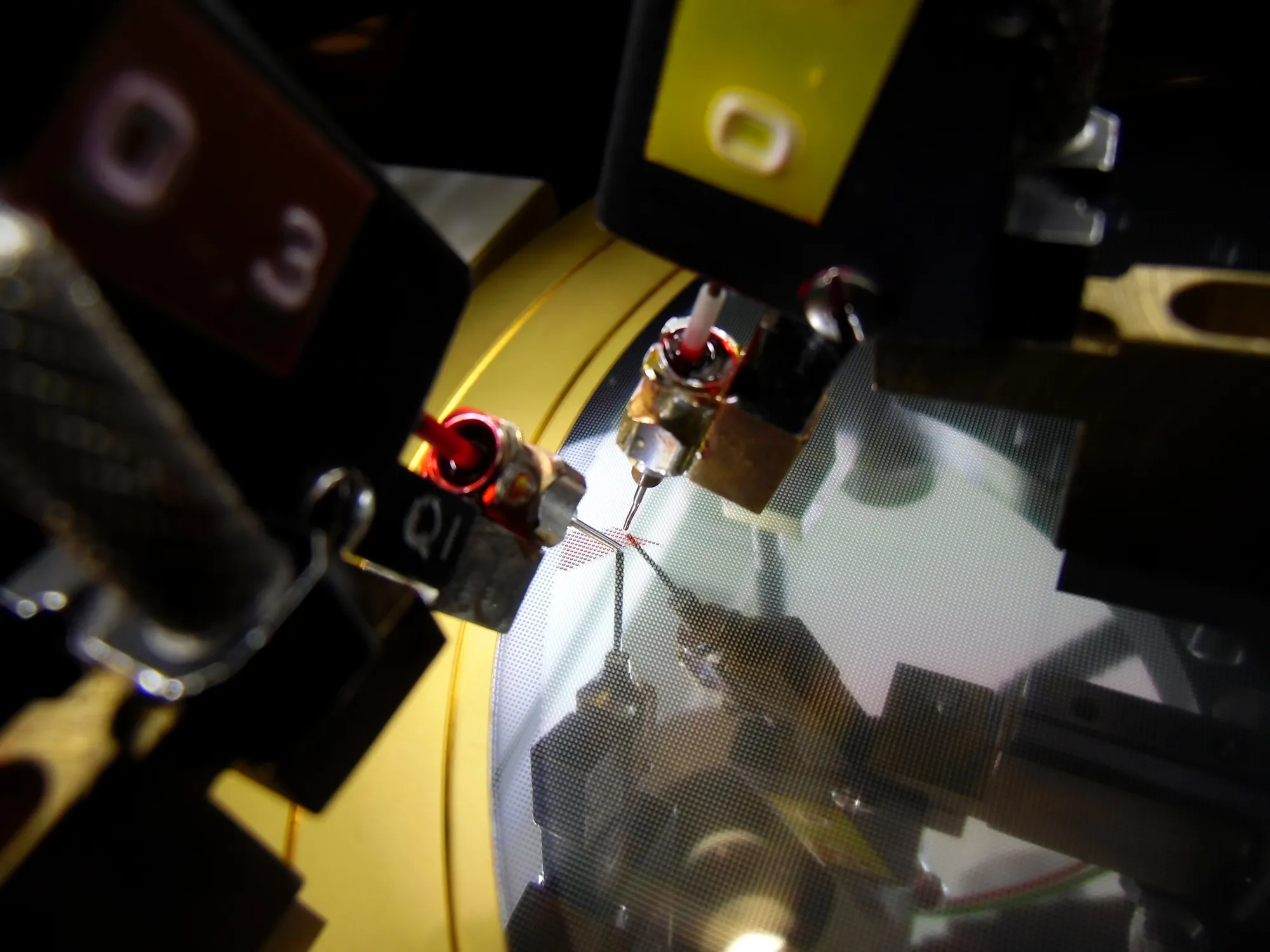
Here is when we learn if the final product is functional or if it needs to be pushed aside for further polishing or perhaps to recycle the materials and start all over again. During the testing process, we expose the ultra-thin wafers to real-world conditions which involve transferring electricity and measuring the rate at which certain particles pass through.
Wafer World has retained its status as one of the premier semiconductor manufacturers thanks to the quality of our products and our position as a thought-leader in the industry. Whether you are in the market for high-quality ultra flat wafers or simply want to learn more about what goes into making semiconductors, you’re already in the right place. Get in touch today for a quote!


