When working with InP reclaim wafers, knowing what constitutes a patterned wafer—and how to specify it correctly—can save weeks of process troubleshooting and significant fabrication costs. Unlike blanket or prime wafers, patterned wafers are defined not only by material quality but also by the pattern on their surfaces and how it aligns with your process goals.
This distinction is especially important in III-V semiconductor environments, where indium phosphide substrates are used for high-speed photonics, radio frequency, and optoelectronic applications.
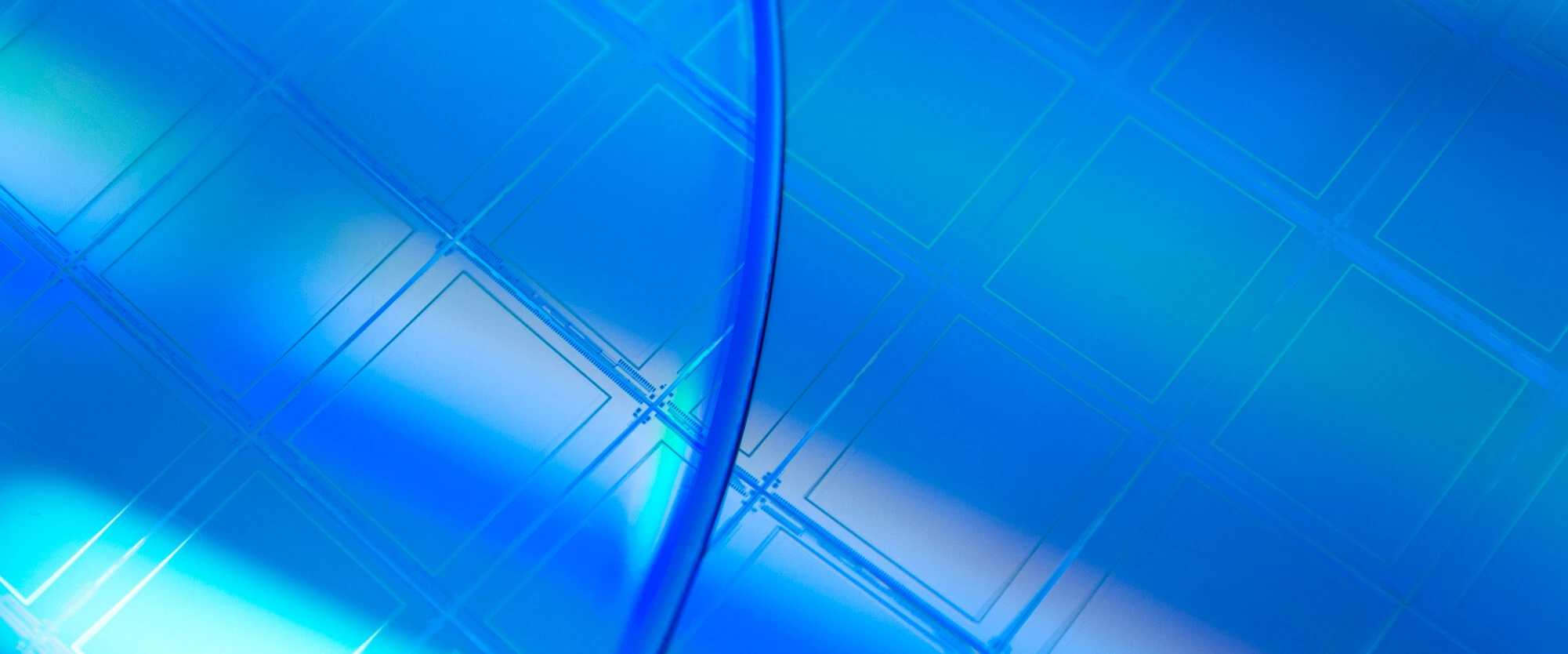
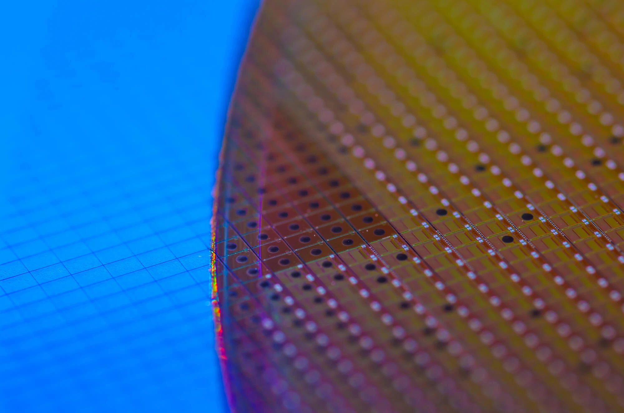
A patterned wafer is a substrate with pre-existing surface features, such as etched structures, alignment marks, dielectric layers, or residual device patterns from previous processing. In the context of InP reclaim wafers, these patterns are typically derived from reclaimed production wafers that have been stripped, polished, and requalified—but not completely blank.
Rather than being a limitation, the remaining features can be a significant advantage for test, development, and calibration tasks.
Patterned InP reclaim wafers are commonly used when the goal is not final device production, but process validation and equipment matching. Typical use cases include:
Because InP substrates are significantly more expensive and fragile than silicon, reclaim wafers offer a lower-cost, lower-risk alternative without sacrificing material relevance.
Not all reclaim suppliers understand how patterned InP wafers are actually used in fabs. Working with a partner who can advise on pattern suitability, limitations, and alternatives helps ensure you order wafers that reduce iteration cycles rather than create new ones.
If your goal is faster process development, better tool confidence, and controlled costs, Wafer World can help. Reach out, and let’s work together to find the best, right-patterned InP reclaim wafer for your project!


