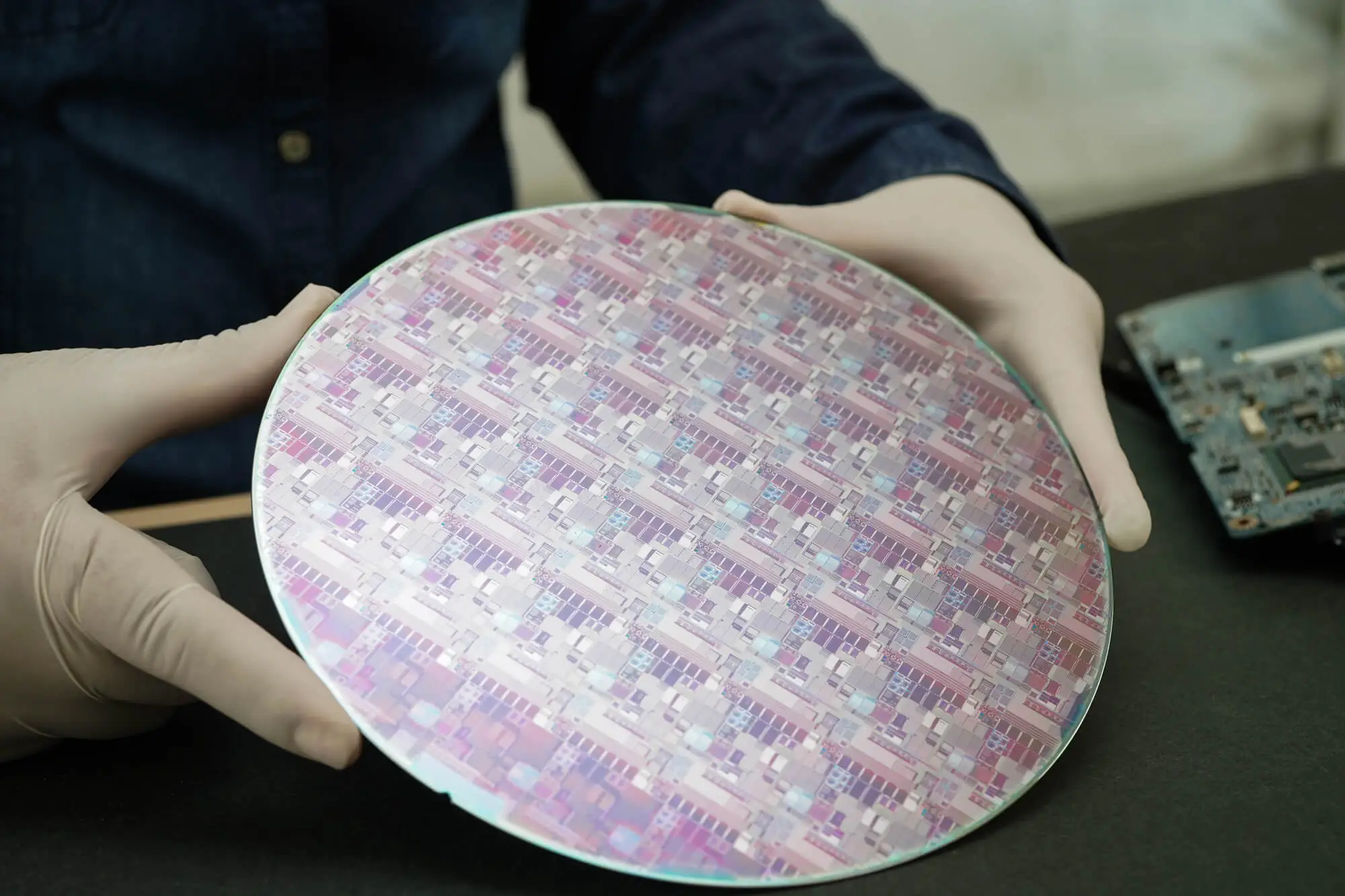
In an industry obsessed with scaling up, the semiconductor world is always looking to develop better, smaller, and more productive chips. For that reason, 450 mm wafers seemed a great innovation: more space equals more places to build on. However, fabs are seeing an unexpected shift: 200 mm ultra-flat wafers are making a comeback, while the long-promised 450 mm generation remains on indefinite hold.
What’s driving this reversal—and what does it mean for manufacturers planning their next capacity investment?
The 200 mm wafer was once the backbone of semiconductor production, powering everything from analog integrated circuits to early microcontrollers. When 300 mm fabs first appeared in the early 2000s, many predicted a rapid phase-out of 200 mm lines. However, by 2025, demand for 200 mm wafers is expected to be higher than ever, driven by the rapid growth of automotive electronics, power devices, and IoT sensors.
These sectors do not require the smallest geometries. What they need are cost-effective, ultra-flat wafers that deliver stable yields and compatibility with mature process nodes.
For more than a decade, the industry chased the dream of 450 mm wafers. Double the diameter promised double the die output per wafer, resulting in major capital gains. Yet, despite major R&D efforts, the economics never lined up.
Equipment vendors are hesitant to invest billions without guaranteed volume adoption. With an industry built around 200 mm and 300 mm wafers, the cost of incorporating new diameters may not be worth the potential profitability.
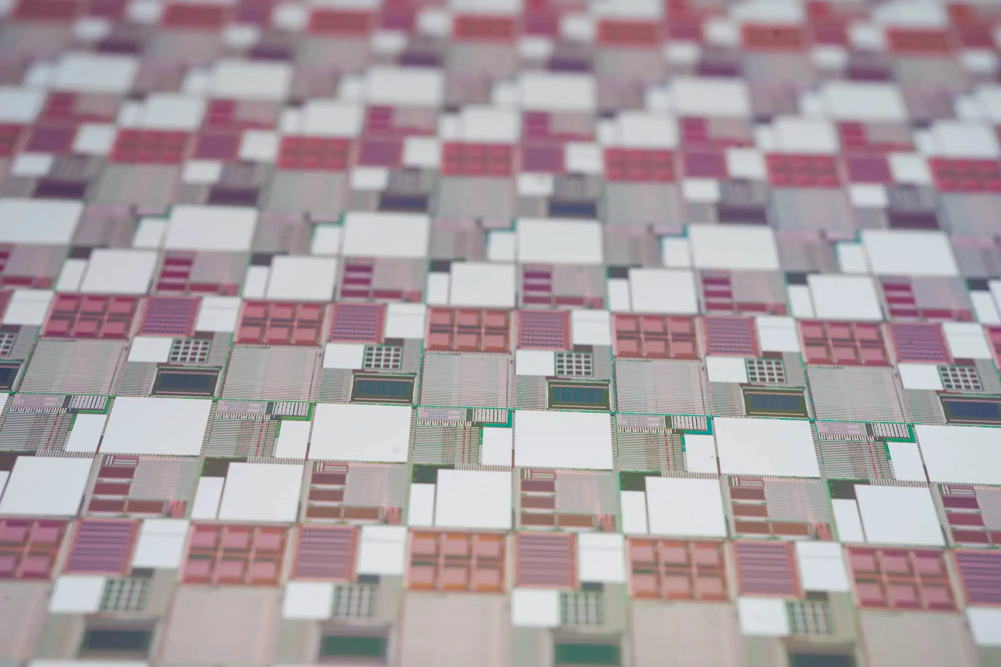
Rather than chasing larger diameters, leading fabs prioritize process control, wafer flatness, and yield optimization. The latest ultra-flat 200 mm wafers now provide planarity tolerances previously reserved for 300 mm production, enabling greater precision in photolithography and improved uniformity in advanced analog and MEMS applications.
After all, innovation isn’t always about scale—it’s about precision, agility, and value. Would you like to experience the benefits of these thin substrates for yourself? Contact Wafer World for more information about our products!


