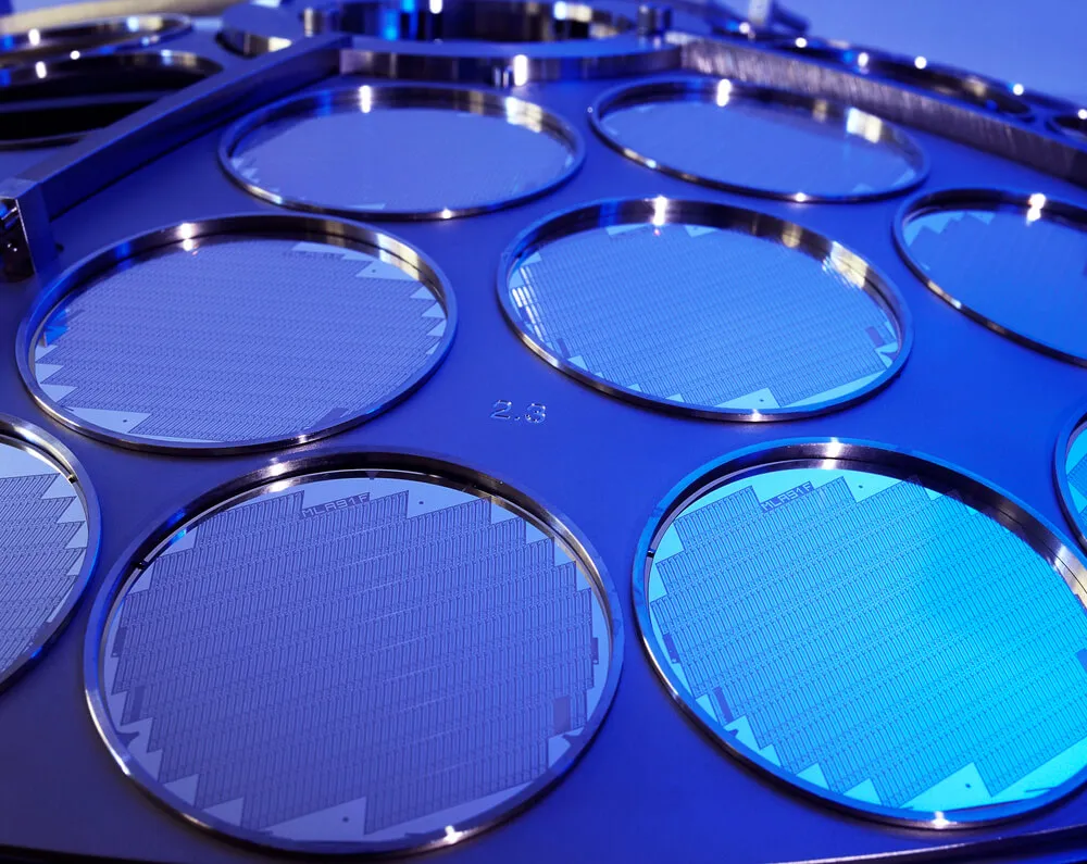
In the world of technology, precision, and miniaturization play a pivotal role in pushing the boundaries of innovation. As electronic devices become increasingly compact and complex, the demand for ultra flat wafers has soared. These wafer-like substrates, often made of silicon, have emerged as key components in various industries, serving multiple functions that are vital to the advancement of modern technology. In this blog post, we will delve into the main functions of ultra flat wafers and explore their significance in shaping our digital landscape.
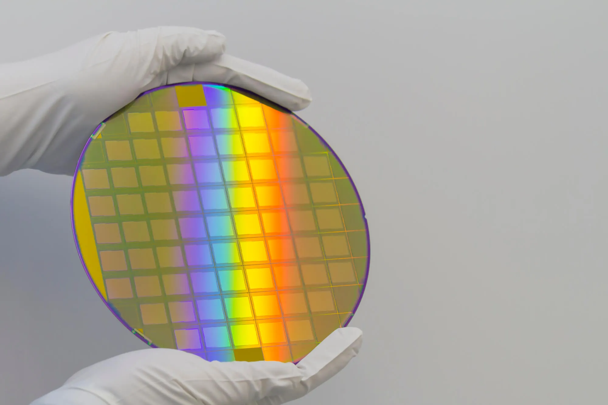
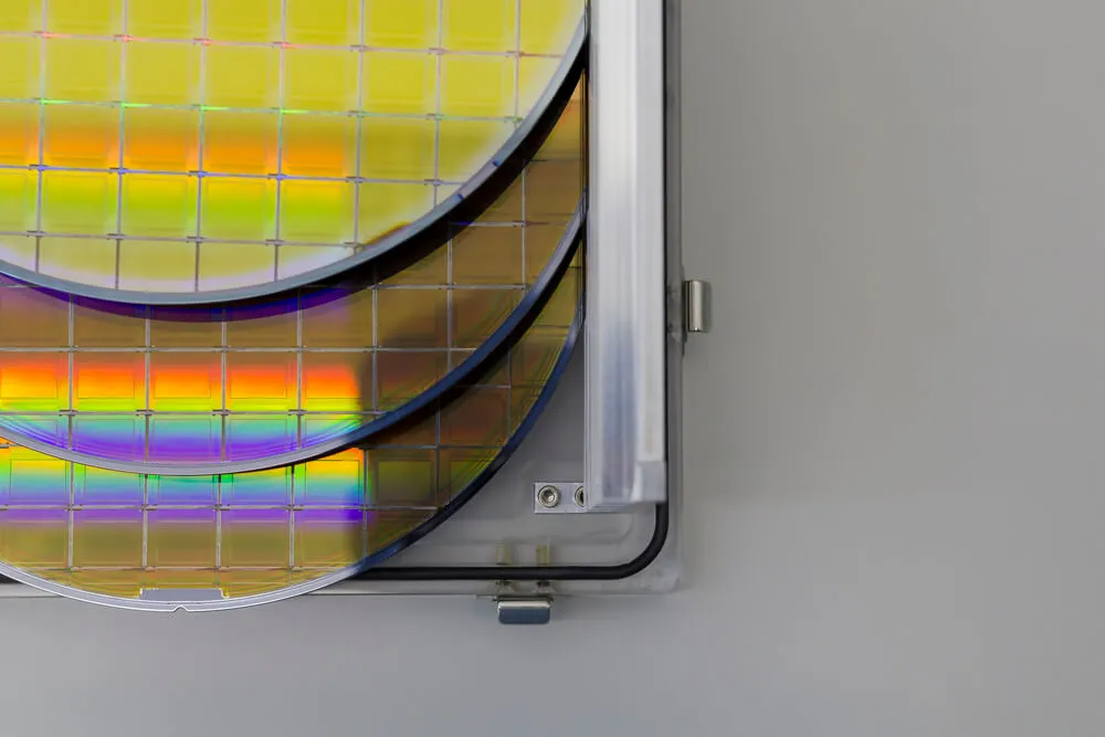
Ultra flat wafers serve as the foundation for manufacturing integrated circuits (ICs) or microchips, which lie at the heart of nearly all electronic devices we rely on today. The wafers provide a pristine surface for the deposition of thin layers of materials, such as silicon dioxide or metal conductors, to create intricate electronic circuitry. Their exceptional flatness ensures uniformity and enables precise patterning of thousands or even millions of transistors, capacitors, and resistors, resulting in high-performance ICs.
Semiconductor fabrication is a complex process involving the creation of electronic components on ultra flat wafers. These wafers act as the canvas for photolithography, where patterns are transferred onto them using light-sensitive photoresist materials. The wafer's flatness is crucial for achieving accurate alignment and dimension control during each step of the fabrication process, ensuring the integrity and reliability of the resulting devices. This capability is particularly vital for manufacturing advanced semiconductor devices, such as microprocessors and memory chips.
Renewable energy sources, like solar power, have gained tremendous traction in recent years. Ultra flat wafers have found a niche in the field of solar cell manufacturing, particularly in the production of thin-film solar cells. These cells are made by depositing layers of semiconducting materials, such as amorphous silicon or cadmium telluride, onto ultra flat wafers. The wafer's flatness allows for uniform and controlled deposition, enhancing the efficiency of solar cell performance by optimizing light absorption and electron flow.
Ultra flat wafers also play a significant role in wafer-level packaging (WLP), a process where individual integrated circuits or chips are packaged together on a wafer before being separated into individual units. WLP provides numerous advantages, such as improved electrical performance, reduced size and weight, and cost efficiency. The flatness of the wafers is instrumental in ensuring reliable bonding, accurate alignment of solder balls or bumps, and effective heat dissipation, ultimately contributing to the overall quality and functionality of the packaged chips.
Ultra flat wafers are indispensable components that underpin the advancement of modern technology. Their exceptional flatness and precise characteristics enable the manufacturing of high-performance integrated circuits, thin-film solar cells, and MEMS devices, and facilitate wafer-level packaging. As our demand for smaller, faster, and more powerful electronic devices continues to grow, the significance of ultra flat wafers will only become more prominent.
Wafer World empowers the digital revolution by enabling the creation of cutting-edge technology that permeates our lives, transforming the way we communicate, work, and interact with the world around us. Call us now to order!


