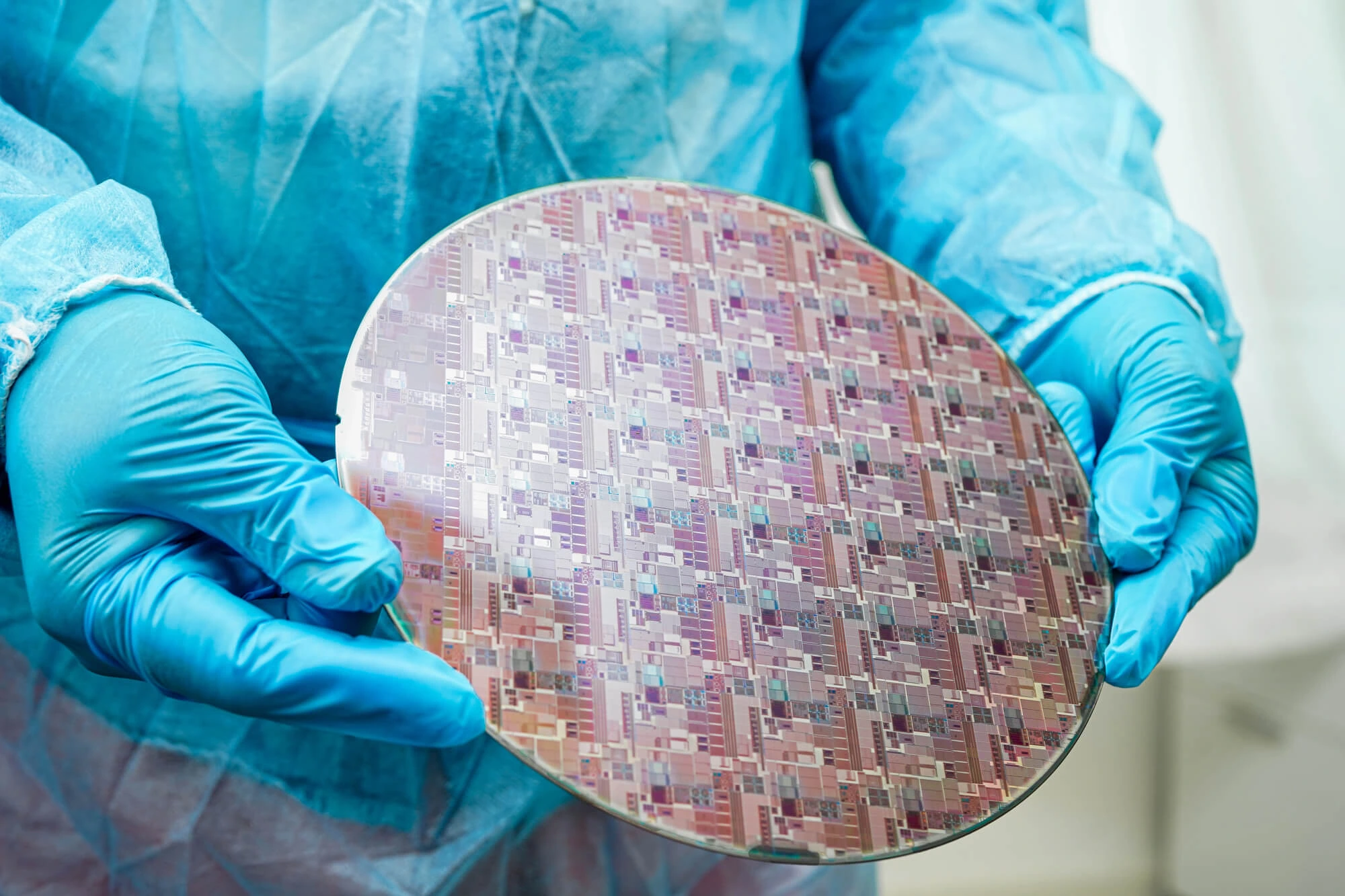
SiO₂ wafers, also known as silicon dioxide or thermal oxide wafers, are silicon substrates coated with a controlled layer of silicon dioxide. This oxide layer plays a critical role in semiconductor manufacturing, MEMS fabrication, photonics, and advanced research applications. Before you buy a silicon wafer, it is essential to understand what SiO₂ wafers are when selecting the right material.
Most SiO₂ wafers are produced through thermal oxidation, a process where high-purity silicon wafers are exposed to oxygen or steam at elevated temperatures. This causes the silicon surface to react and form a dense, uniform layer of silicon dioxide that is tightly bonded to the substrate.
Thermal oxide layers are valued because they offer:
Depending on the application, oxide thickness can range from a few nanometers to several microns, making SiO₂ wafers highly customizable.
Silicon dioxide is not just a protective coating—it is a functional layer that enables many modern device structures. In integrated circuits, SiO₂ serves as both an electrical insulator and a passivation layer, preventing leakage currents and protecting devices from contamination. In MEMS and sensor applications, it can serve as a sacrificial layer, a structural layer, or a surface treatment to enhance sensitivity and reliability.
Due to its optical transparency and predictable refractive index, SiO₂ is also widely used in photonics and optoelectronics, including waveguides and thin-film applications.
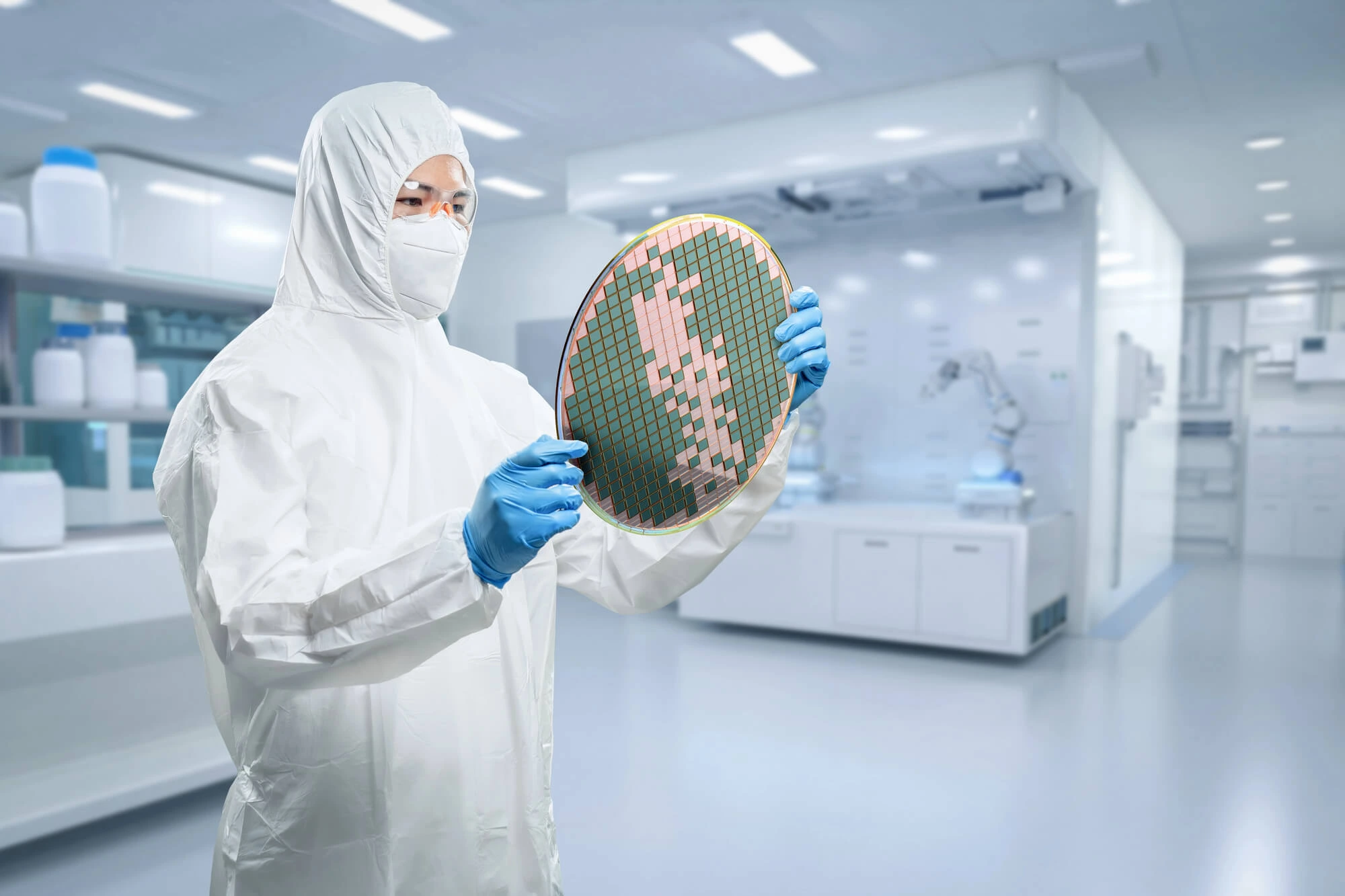
SiO₂ wafers have become a valuable asset in modern semiconductor and microfabrication processes. Their electrical insulation, chemical stability, and process flexibility make them suitable for a wide range of applications.
When evaluating options to purchase silicon wafers, selecting the right product for your project directly impacts device yield, reliability, and overall project cost. Contact Wafer World, and let’s find the perfect substrate for you!


