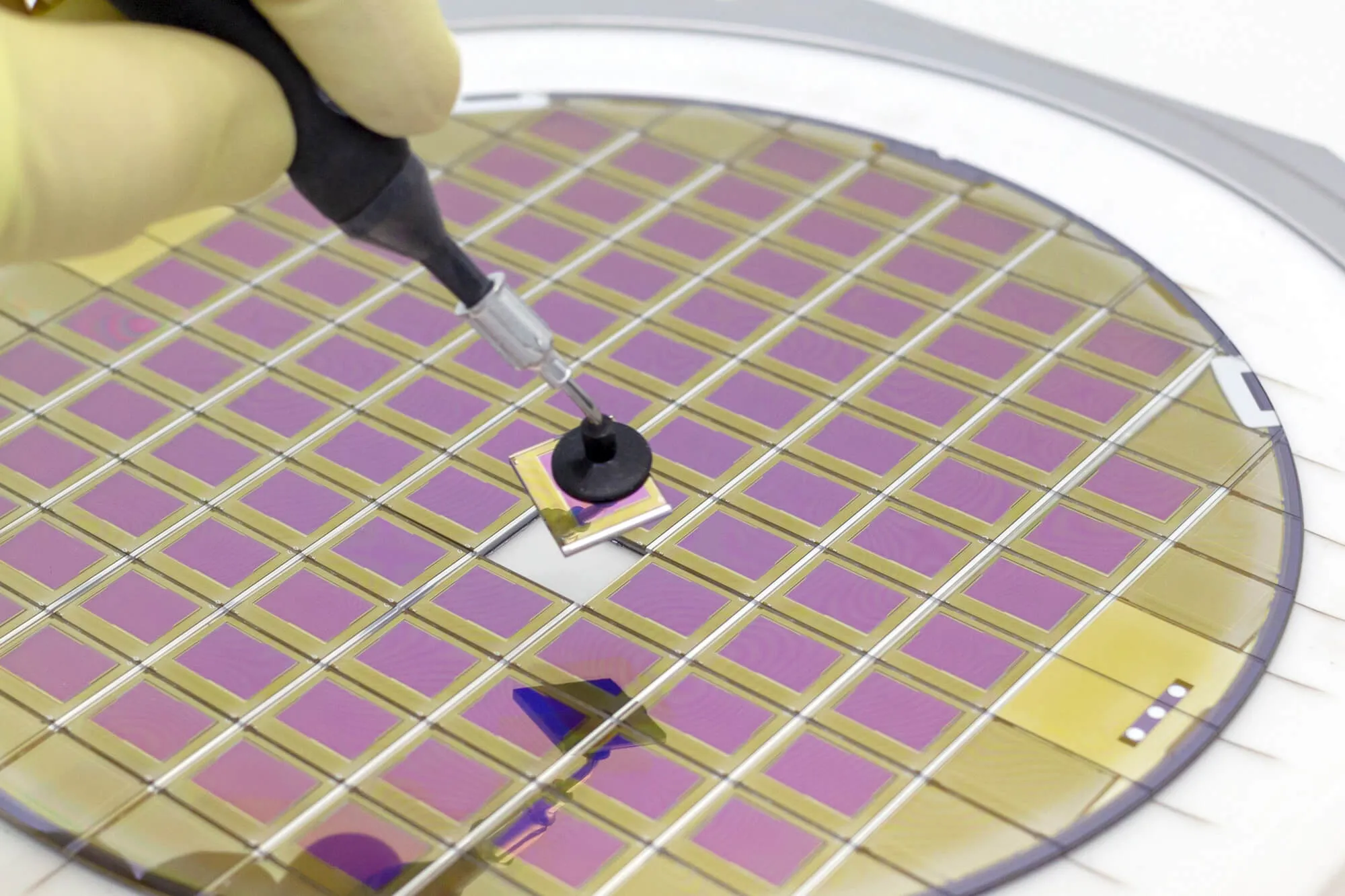
Did you know that laser marking technology plays a critical role in silicon wafer manufacturing? It involves the use of a machine that’s specifically programmed to emit a beam of concentrated light particles to put marks on semiconductor packages. Without this technology, it would be impossible to track the wafers throughout the entire manufacturing process.

Since the process of marking silicon wafers is completely automated, it takes away the variable of human error and ensures the absence of human interaction with the lasers. Each wafer is handled and transported by a mechanical arm until the markings are completed.
The markings on thin silicon wafers are usually less than a millimeter tall. However, thanks to its high level of precision at constant quality, superior laser technology can mark extremely small geometries and 1-point fonts. Since these markings are clearly legible, they make it easy for computers to track the semiconductor packages during the manufacturing process.
Besides being extremely precise, this laser technology is also known for being the fastest marking process that’s available in the market. Its high marking speed allows manufacturers to increase their productivity while reducing the cost of production. In just a matter of minutes, multiple stacks of silicon wafers can be laser marked.
One of the best things about using laser technology in marking silicon wafers is that it doesn’t strip away the wafer’s surface layer. Except for a slight color change beneath its surface, the laser-marked wafer’s perfect condition is preserved.
Laser parameter settings can produce permanent and durable markings that are resistant to heat, abrasion, and acids.
If you’re looking to find an eco-friendly way to mark semiconductor packages, laser technology is your best bet. Unlike other marking methods, it doesn’t make use of inks and other toxic chemicals. What’s more, marking silicon wafers via laser technology doesn’t require the use of much energy.

At Wafer World, we strive to provide our customers with the highest quality, laser-marked silicon wafers. Feel free to contact us today for inquiries.


