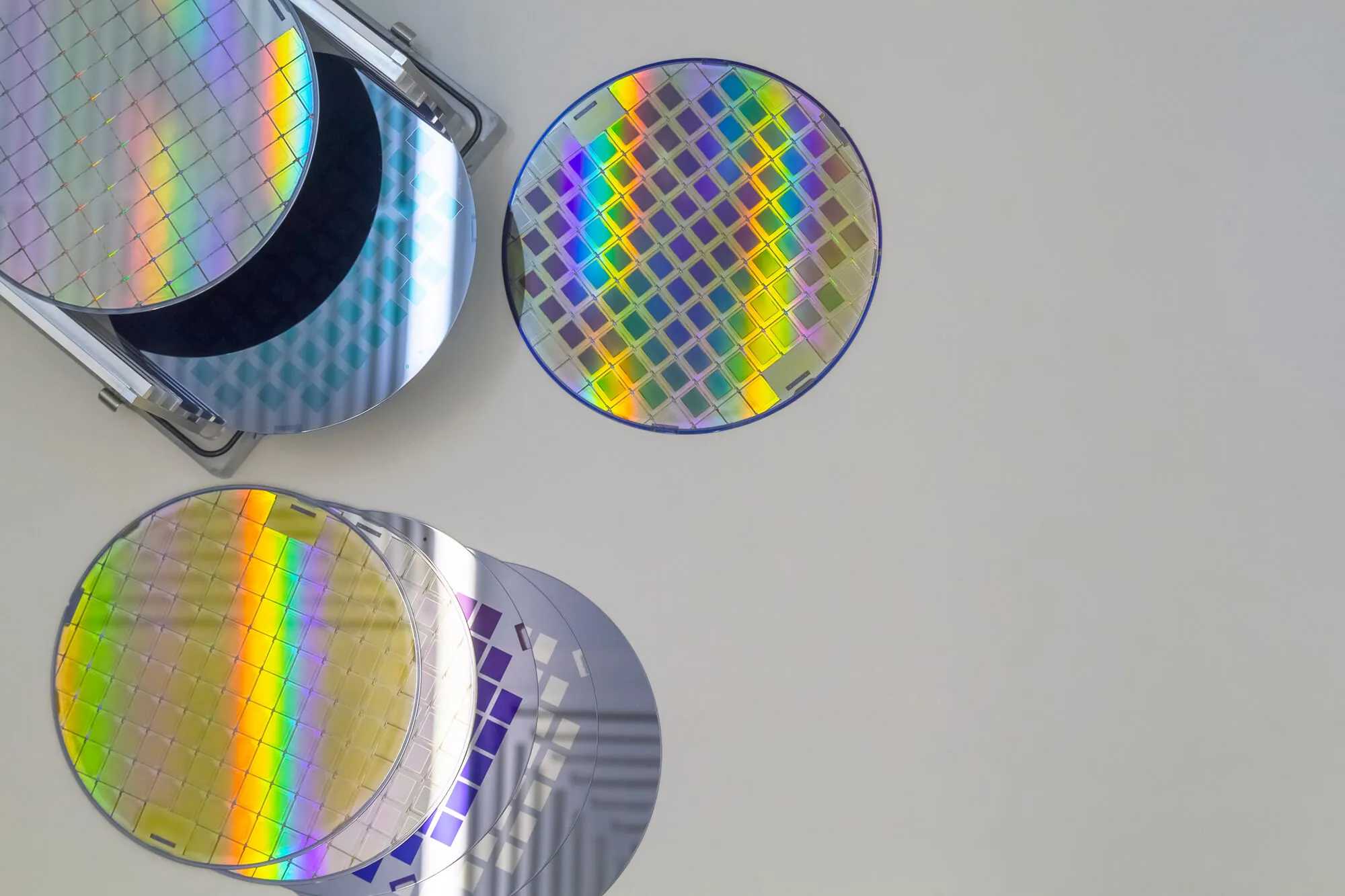
While you may be familiar with the Czochralski process, how much do you know about float zone wafers (FZ)? These high-quality alternatives undergo an entirely different approach which also results in ultra-pure wafers with various uses.

FZ wafers are purer than Czochralski (CZ) counterparts and achieve their purity much quicker. These wafers have since been used liberally for endeavors ranging from submarine missions to smart cars. The possibilities are endless, yet the story starts before their creation. In the early 1950s, a term came into being known as “zone melting.” Occurring during purification of any given element but also used to manipulate its composition as well. You’d achieve this by melting a localized area, causing the liquid zone to travel slowly through a long and narrow ingot, shedding impurities along the way. This is how it achieves its near perfection. After zone melting, the given element or compound can undergo what’s known as “zone refining.” Over the last 70 years, elements such as germanium and silicon have been refined in this way, resulting in wafers with one part impure out of the 10,000,000,000 parts germanium.
Looking ahead to 1962, Henry Theurer turned the zone melting process into the wafer manufacturing method still in use today. While there are many uses for float zone wafers, Theurer benefitted every modern-day solar panel user and a few other industries. What makes them superior in this application is their greater growth rate when compared to CZ wafers. On average, these are 2-3x larger, which contributes to their purity. However, oxygen places a key role as well. Between the high heat and growth rates, FZ versions contain far less oxygen. The more O2 in a wafer adversely affects its life expectancy. However, this is usually only concerning when the application is for solar or other niche energy power supplies. For more everyday use, you won’t notice as drastic of a reduced life span. The dopant process is crucial for solar panel application. For doping FZ and CZ wafers, n-type dopants evaporate during melting. Their dopants are typically phosphorous or other electron donors to create an extrinsic semiconductor. Lastly, these have five electrons, one more than before the doping process. Conversely, solar panel semiconductors are p-type doped with boron, indium, or gallium, which strip electrons away. This void creates a positive charge whereas n-types of negative. These dopants allow the semiconductor to be more resistant to degradation caused by overexposure to sunlight.
FZ wafers have a wide array of uses in various gizmos, such as computers, tablets, smart cars, radios, and televisions. Float zone wafers are a component of BJTs (bipolar junction transistors) and have been so since the late 1940s, courtesy of William Shockley, John Bardeen, and Brattain. These inventors didn’t just create a product. They revolutionized technology, paving a path to our ever bright future. Not only that, this is a remarkable invention, as it affects nearly everyone worldwide daily. All of the everyday gizmos you’ve grown accustomed to using have been made possible by these three individuals. The reason BJTs have been so effective at amplifying signals because they don’t use an n-type or a p-type semiconductor. Instead, BJTs use both, which grants it the ability to use phones and radio broadcast towers. The reasoning for the name bipolar is because at either end is an oppositely charged conductor containing a collector and an emitter. As the current flows through one end, the opposite emitter changes the current pattern. As it turns out, channeling signals through both semiconductors is more efficient.
FZ wafers continue to benefit modern lights or non-Edison bulbs. However, when the origin of the lightbulb comes up in conversation over dinner with family, many claim Thomas Edison was the inventor in 1879. However, shocking the masses, he wasn’t the inventor. Various lightbulbs inventions sprinkle the 19th century, namely in the history of Britain. The two competing forms were ARC and incandescent, and after 60 years of battling, incandescent won out due to Edison’s contribution. Instead of inventing the bulb, he made the production process easier and faster, leading to a better the bulb. The critical difference between the two bulbs is how they generate light. ARC technology relies on arced electrical current to cover a gap between two electrodes. The heat generated burned off in the form of visible light. However, Humphry Davys’ 1802 invention glowed far too bright and too short-lived for consistent daily use. Edison, however, improved the electrical bulb variation, which does not combust. Instead, a thin wire is heated to the point of incandescence while inside a vacuum. The absence of oxygen prevents sparking. Later on, Edison found that bamboo would last up to 1200 hours of use, which was in use until fluorescent and LED bulbs. In the infancy of the float zone wafer, the LED bulb made its debut courtesy of scientist Nick Holonyak Jr. Done so on accident. He was trying to craft a visible laser while General Electric scientists were busy working on an infrared laser. Mere weeks before Holonyak Jr debuted his semiconductor laser; the GE scientists had theirs released. The follow-up by Nick radiated red, the telltale glow of gallium arsenide phosphide. While not a tight beam of light he was after, the radiating light sparked widespread uses seen today. Everyday devices that use LED bulbs aren’t limited to:
The very object Nick Holonyak Jr tried to craft utilizes light-emitting diodes as well as FZ wafers. Lasers are no more than a highly concentrated beam of light. Did you know laser stands for light amplification by stimulated emission of radiation? Since its introduction, more industries have begun to integrate lasers into their processes. Currently, they have residential, commercial, military, and governmental use. Here are a few ways lasers currently benefit society:

No matter what brought you into the market for FZ wafers, we have been manufacturing them since 1997. Regardless of your wafer needs (inp reclaim, GaAs, Silicon, etc.), we can help guide you to what exactly you need. Contact us today for a quote.


