Do you know how important semiconductors are? They are actually crucial! So much that you probably can’t live without them–or wouldn’t want to. Before you scratch your head in confusion, try to look at what you’re holding. Is it a smartphone? Where are you reading this from? Is it from your laptop or tablet? If you are, then you definitely want semiconductors in your life. Specifically, we are going to dive into the world of an Si Wafer. But let’s back up.Semiconductors are used to make microchips in electronic devices such as televisions, video games, radios, computers, and smartphones to name a few. Over the last 5 decades, semiconductor technology has evolved allowing manufacturing companies to produce reliable, small, and fast devices. One of the most popular semiconductors in the world is an Si Wafer.

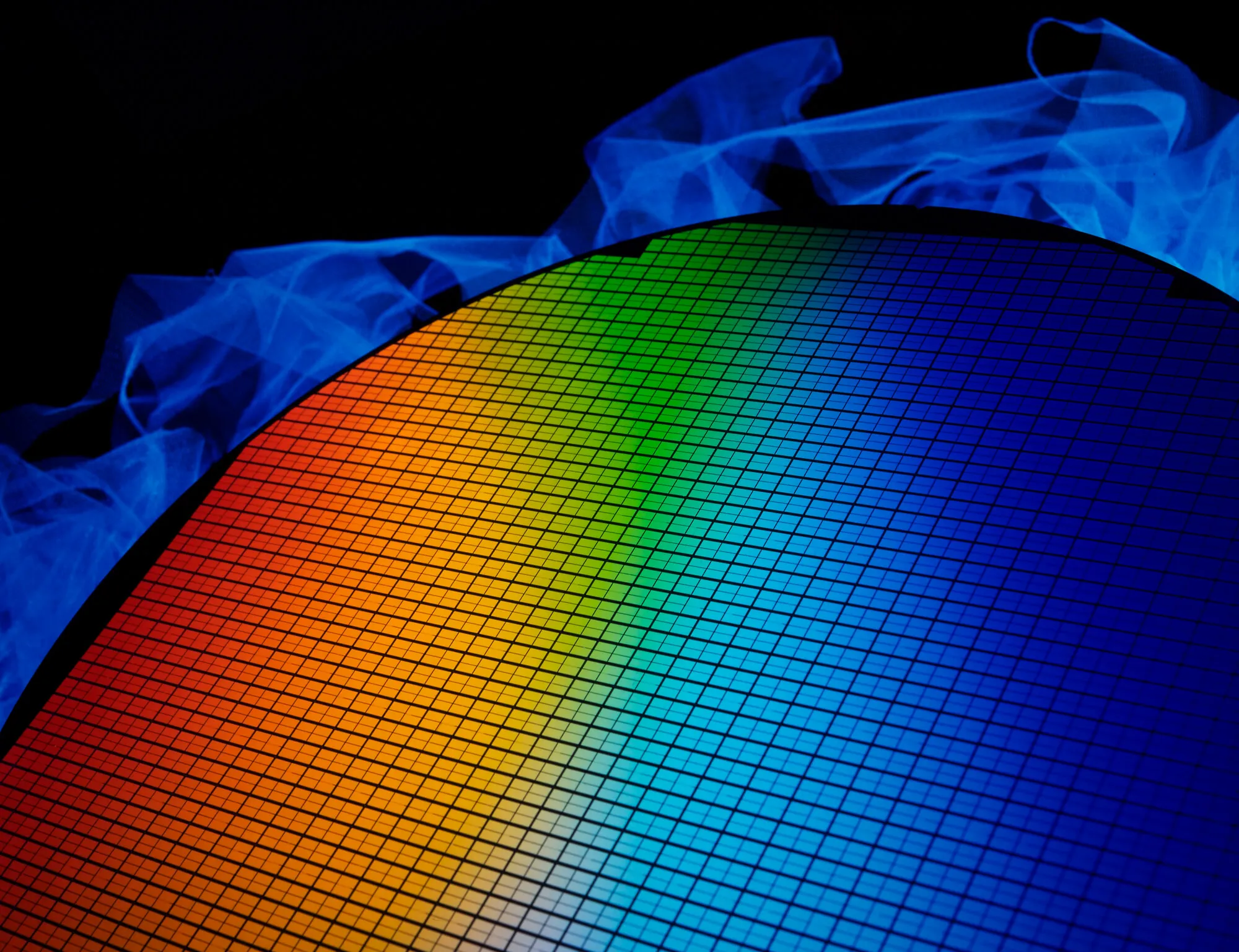
An Si Wafer, or silicon wafer, is popularly used in creating semiconductors. Semiconductors are present in all kinds of electronic devices, including smartphones and desktop computers. Did you know Silicon is also one of the most common elements on the planet? Literally, in its wafer form, it’s a thin, flat, mirrored disk.Furthermore, the surface has very few irregularities due to its extended purification process–also making them exceptionally clean. They are cleaned of all micro-particles and impurities making them an ideal substrate used in semiconductors.Fun Fact: A silicon wafer is also hailed as the flattest object in the world. Crazy, right?
The Si Wafer manufacturing process involves several steps before it can become a semiconductor.

Are you looking for a trustworthy company that manufactures high-quality silicon wafers? Wafer World is hailed as the leader in silicon wafer manufacturing. We serve customers in more than 40 countries. If you want to learn more about our company, visit our website!


