Indium Phosphide (InP) is one of the most important compound semiconductors in modern electronics, essential for high-speed, high-frequency, and optoelectronic devices. But why is that? To understand why an InP wafer exhibits such unique electrical behavior, it is helpful to start with the basics, which include learning the atomic numbers of its elements.

Indium phosphide is composed of indium (In) and phosphorus (P) atoms.
When these two elements combine in a 1:1 ratio, they form Indium Phosphide (InP)—a III-V compound semiconductor (from groups III and V of the periodic table).
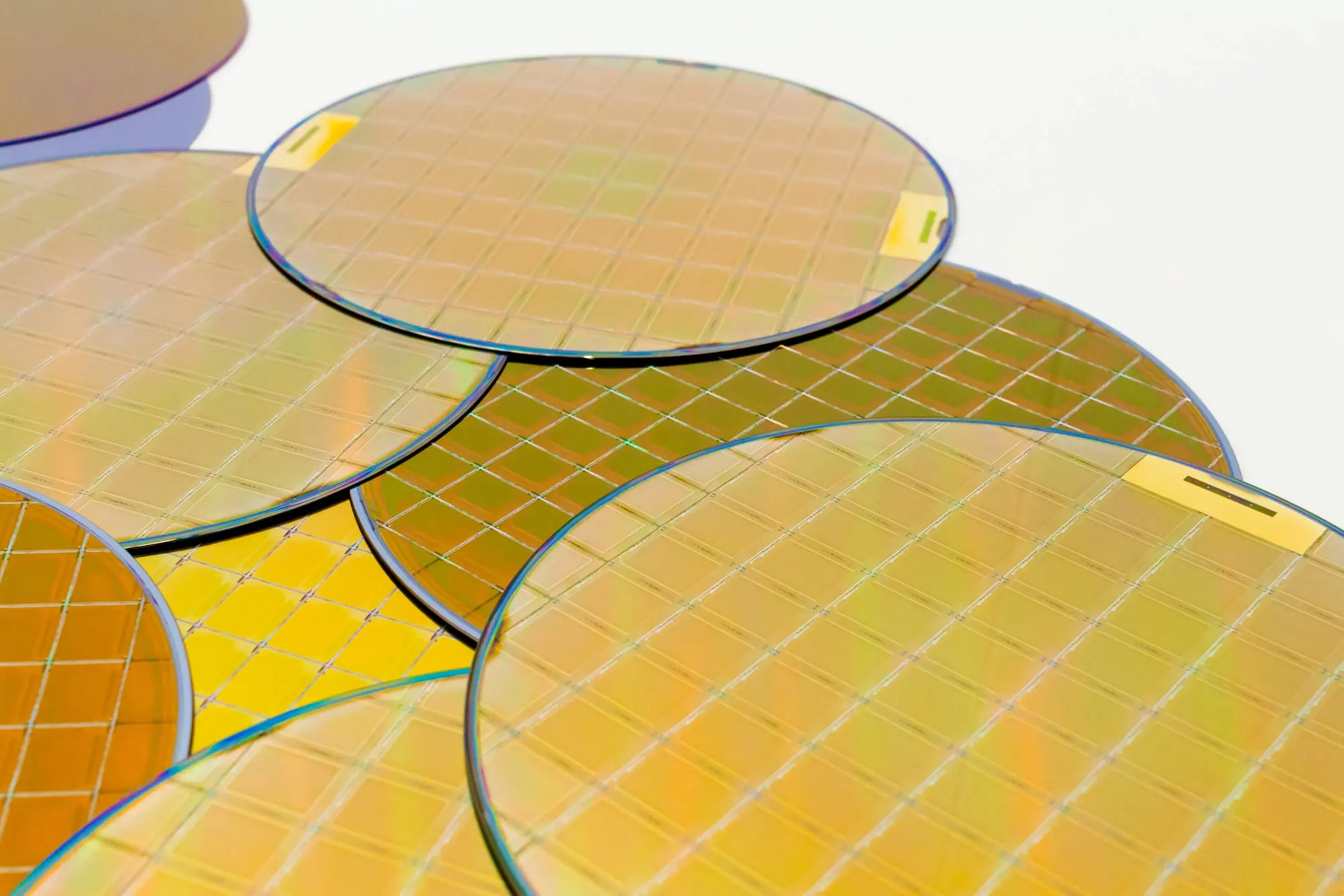
This balanced structure gives InP its remarkable physical and electronic properties—high electron mobility, a direct bandgap, and excellent thermal stability—making it ideal for use in InP wafers for advanced photonic and RF applications.
Compared to silicon (Si) or gallium arsenide (GaAs), InP wafers offer superior electron velocity and lower noise—critical advantages for terahertz and optical communication technologies.
On the other hand, InP has a direct bandgap of 1.34 eV at room temperature, which allows for efficient photon emission and absorption, making it ideal for lasers and photodetectors, high-frequency transistors, solar cells, photonic integrated circuits, and more.
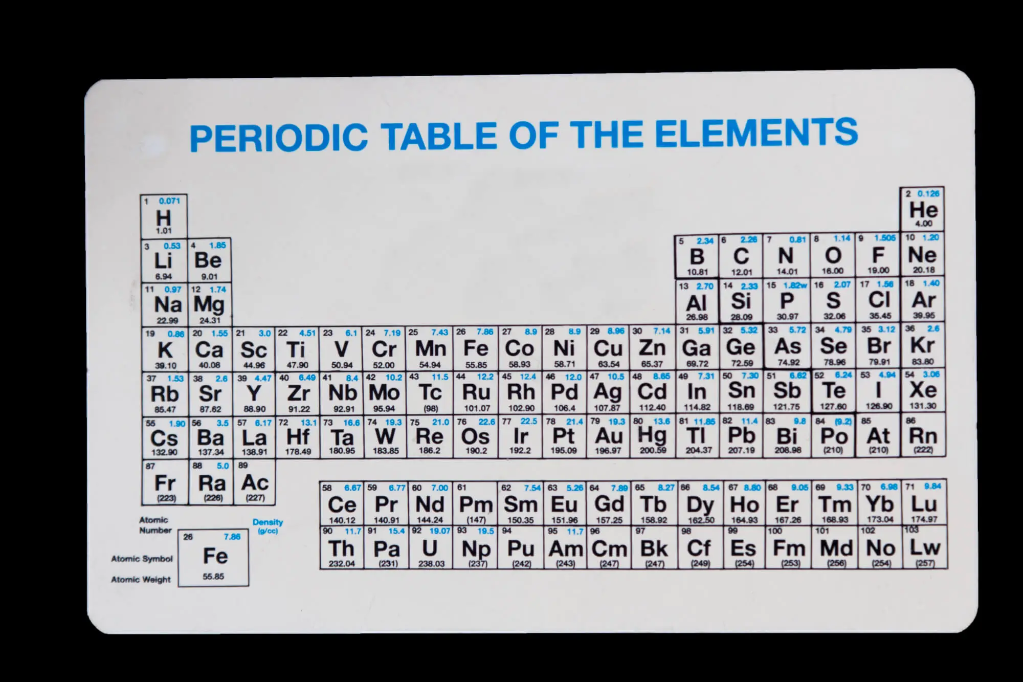
For wafer manufacturers, understanding atomic and electronic structure directly translates to improved performance. The atomic numbers of indium and phosphorus determine the electron configuration and bonding characteristics that make InP stand out among compound semiconductors.
Would you like to experience these advantages for yourself? Contact Wafer World—we offer small batches, adapted to research & discovery needs!


