N-type silicon is crucial in modern semiconductor manufacturing, enabling faster devices, higher efficiency, and enhanced electrical performance in various applications.
Understanding how N-type silicon is used—from power electronics to advanced sensors and solar cells—helps clarify which material fits each application.
By selecting the right option recommended by silicon wafer manufacturers, engineers and procurement teams can choose the best wafer for their process and avoid costly design compromises.

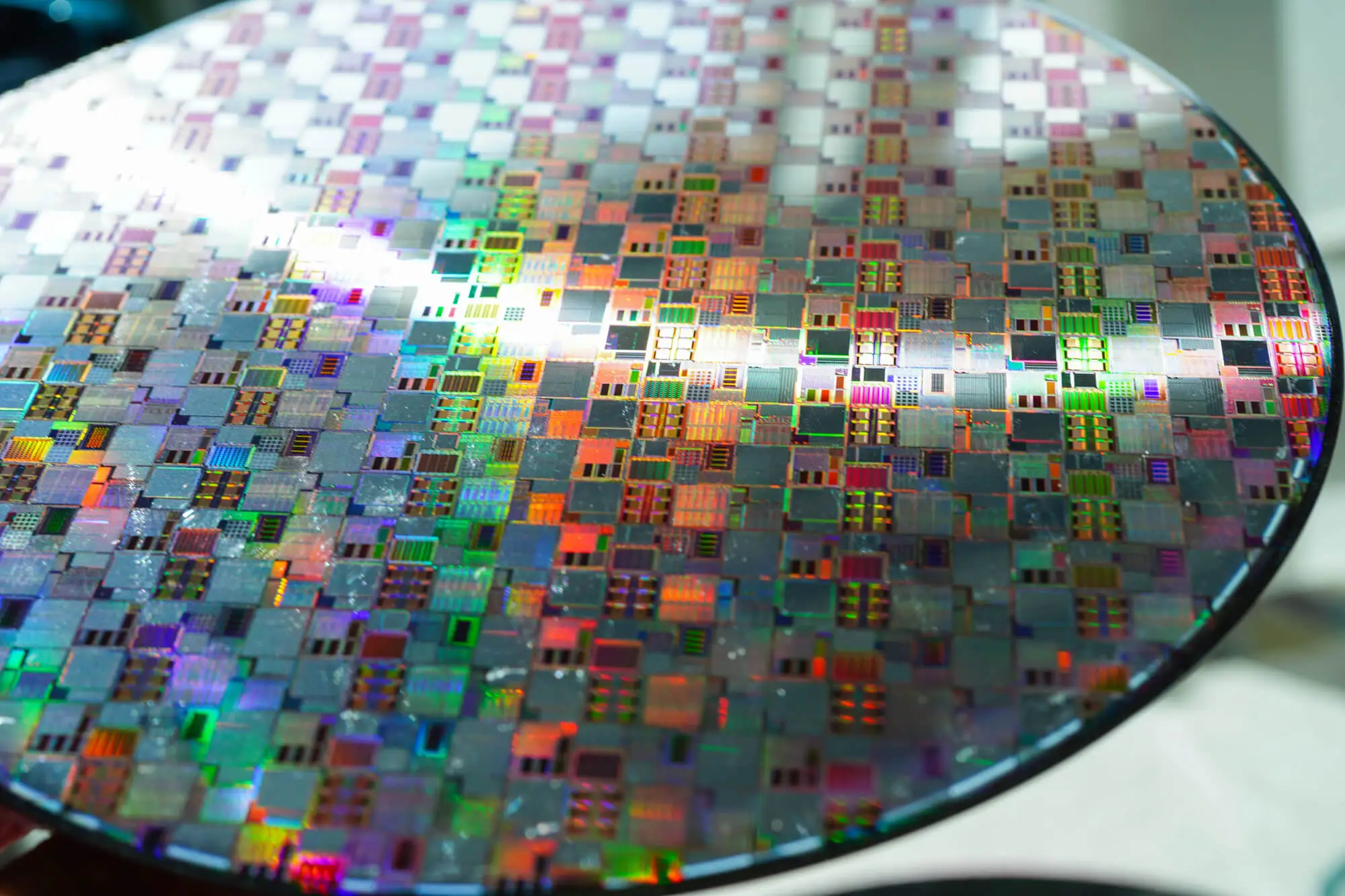
N-type silicon is created by doping high-purity silicon with donor elements such as phosphorus, arsenic, or antimony. These dopants introduce extra free electrons, making electrons the majority charge carriers. Compared to P-type silicon, N-type materials typically offer higher electron mobility, lower resistive losses, and more stable electrical behavior under high-field conditions.
Due to these characteristics, N-type silicon wafers are widely specified when performance, efficiency, and reliability are most important.
Common applications of these types of silicon include:
One of the most important uses of N-type silicon is in power MOSFETs, IGBTs, and diodes. The higher electron mobility of N-type substrates supports lower on-resistance and improved switching efficiency, making them ideal for electric vehicles, power supplies, and industrial automation systems.
N-type silicon is fundamental to CMOS fabrication, where N-type and P-type regions work together to form transistors. In advanced nodes, tightly controlled N-type doping enables better drive current, improved speed, and reduced power consumption—key requirements for CPUs, GPUs, and mobile processors.
In photovoltaics, N-type silicon wafers are increasingly preferred for high-efficiency solar cells. Compared to traditional P-type wafers, N-type substrates are less sensitive to light-induced degradation (LID), resulting in improved long-term performance and higher energy yield.
N-type silicon is widely used in image sensors, photodetectors, Hall-effect sensors, and MEMS devices. Its low noise characteristics and stable electrical properties improve sensitivity and measurement accuracy, particularly in optical and sensing applications.
Not all N-type wafers are the same. Leading silicon wafer manufacturers offer control over:
Choosing the right combination ensures your wafer aligns with both device design and fabrication requirements.

N-type silicon is utilized in applications where performance, efficiency, and reliability are crucial, including power electronics, solar energy, advanced integrated circuits, and sensors.
By understanding its benefits and collaborating with experienced silicon wafer manufacturers, you can select the optimal N-type substrate for optimal device performance and production yield.
Wafer World offers a wide range of specifications, tight tolerances, and technical guidance. Contact us to learn more!


