
In semiconductor manufacturing, precision and surface integrity are essential. Two critical processes used for surface modification and laser marking are wafer etching and annealing. While both of these procedures employ lasers—and both share the common goal of altering the wafer’s surface properties with extreme accuracy—their underlying mechanisms and effects on the material are fundamentally different.
Understanding these differences is crucial for selecting the appropriate process for specific applications in microelectronics, photonics, and materials engineering.
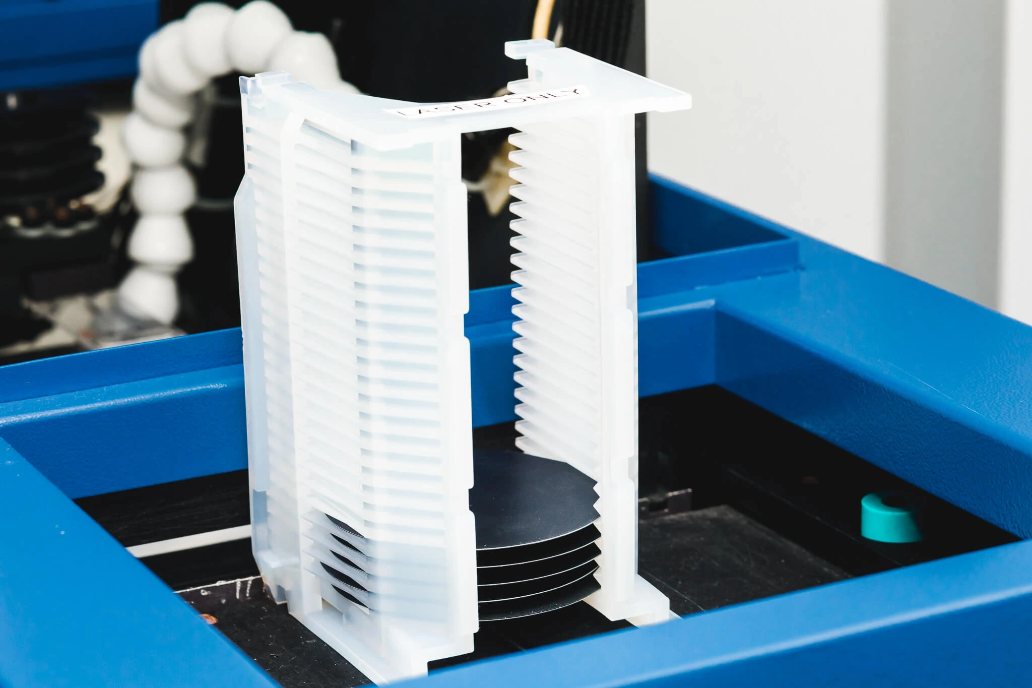
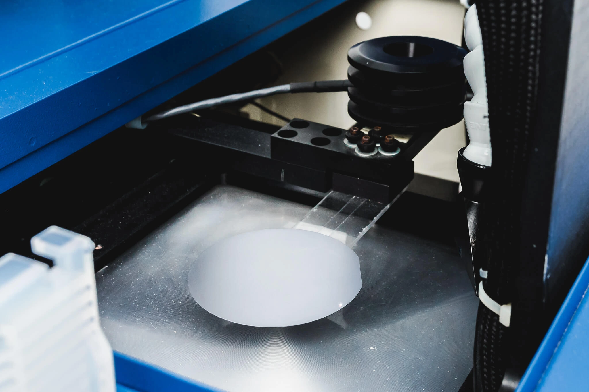
Etching, often referred to as laser ablation, is a material removal process. In this method, a high-energy laser beam is directed at the wafer surface, where the energy is absorbed and converted into heat.
The rapid, localized heating causes the target material to vaporize or sublimate, effectively removing it layer by layer according to a programmed pattern. Other advantages include:
The process is entirely non-contact, reducing the risk of contamination or mechanical stress on delicate substrates.
Annealing, by contrast, is a non-destructive surface modification process that changes the material’s microstructure without removing any material. Instead of reaching vaporization temperatures, the laser heats the surface to a level below the material’s melting point.
This controlled heating alters the crystalline structure of the material or induces the formation of a thin oxide layer. The result is:
While etching and annealing have their differences, they both offer substantial benefits over conventional marking and machining techniques. Mechanical scribing, for example, can introduce microcracks and surface stress, compromising wafer performance and yield. Ink-based marking can degrade under heat or chemical exposure, reducing durability.
Instead, laser-based methods deliver superior process tolerances, cleanliness, and long-term reliability—which is why we continue to reinforce them at Wafer World. If you’d like to learn more about our manufacturing techniques, reach out today for more information!


