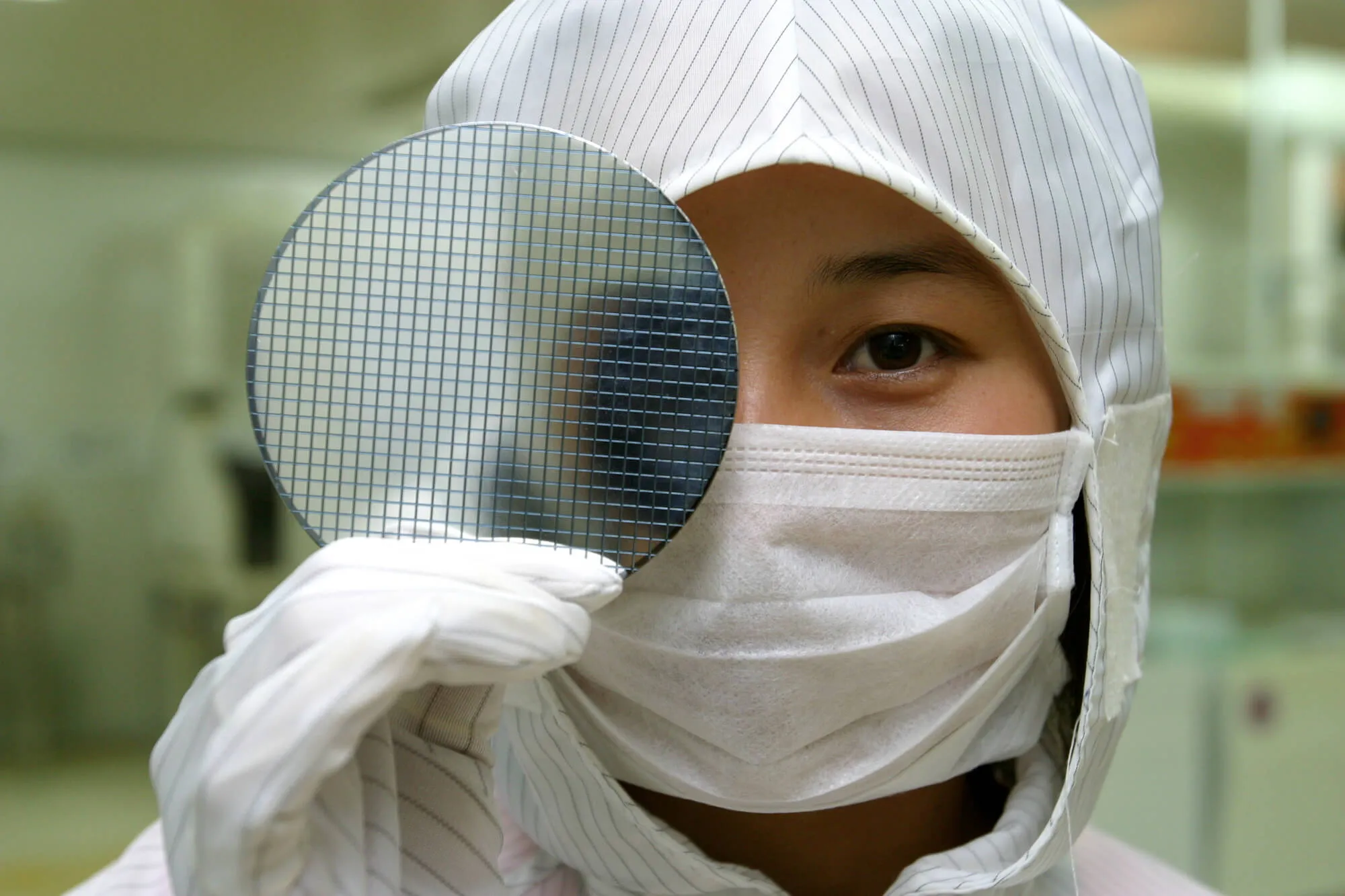
Portable and lightweight gadgets like smartphones, USB memory sticks, and handheld music players are still being introduced by modern technology. Developing these would not be possible without reducing the size of their components. For this reason, the backside of wafers must be thinned before wafer dicing to produce thin silicon wafers.
Mechanical grinding, chemical-mechanical planarization (CMP), wet etching, and atmospheric downstream plasma (ADP) with dry chemical etching are all techniques for wafer thinning (DCE). However, traditional grinding and chemical-mechanical planarization are the two most popular techniques for wafer thinning. If you want to learn more about this topic, here's everything you need to know about wafer thinning.
Wafer thinning, often referred to as wafer backgrounding, is a process used to fabricate semiconductor devices in which the thickness of the wafer is decreased to enable integrated circuit stacking and high-density packaging for small electronic devices.
Therefore, thinning removes material from a wafer's backside until the appropriate target thickness is eventually reached. The wafer backgrinding procedure aims to remove a specific amount of material by grinding the wafer's substrate material, typically silicon. It benefits chip size specifications, heat dissipation, and requirements for the device packaging process.
Wafer shrinking is a crucial step to achieve this since ultra-compact electronic goods like microchips and portable gadgets need tiny components. Electronic gadgets, which get smaller with each new design, may fit smaller and more compact circuits made from thinner silicon wafers, typically lighter and smaller.
In general, electronic inventions progress by improving performance while becoming lighter than their predecessors. As a result, for more components to fit into these devices, semiconductors must be smaller, more densely packed, and lighter in weight to make place for additional components. Because of this, wafer grinding is a crucial step in producing semiconductors.
At Wafer World, our team can provide you with high-quality thin silicon wafers for your business. Contact us to learn more about the products we provide!


