.jpg)
Stay up-to-date with the latest news and trends in wafer and semiconductor technologies.
*Blogs are for educational and informational purposes ONLY

Laser marking is a key step in silicon manufacturing, but it can be dangerous and affect product quality if the right safety measures aren’t taken.
Read More
To ensure the surface of a Si wafer is free of flaws, manufacturers employ various surface control methods. Here, we’ll go over them, exploring their use and advantages.
Read More
Smartphones use several thin silicon wafers to perform all of their functions perfectly, but have you ever wondered how many of them there are?
Read More
Our General Manager, Ronnie Phelix, has been nominated by the SFMA for Employee of the Year. We want to say congratulations, Ronnie, from everyone at Wafer World!
Read More.jpg)
To manufacture a GaAs wafer, gallium and arsenide first must be procured. Here, we’ll explore how GaAs is crafted—and if the USA can make it domestically in the future.
Read More
An InP wafer can find several uses, but it’s currently used in large quantities in quantum computing. Here, we’ll break down why.
Read More
Assessing the electrical properties of a material is crucial during silicon wafer manufacturing. Here are some of the key factors to look at.
Read More
An FZ wafer is a safe material in its final solid form, but incorrect handling can be toxic and cause serious health problems, and here, we’ll explain why.
Read More
Lately, oversupply and decreased demand have made silicon prices drop—however, new tariffs could reverse this trend in the future, and here’s why.
Read More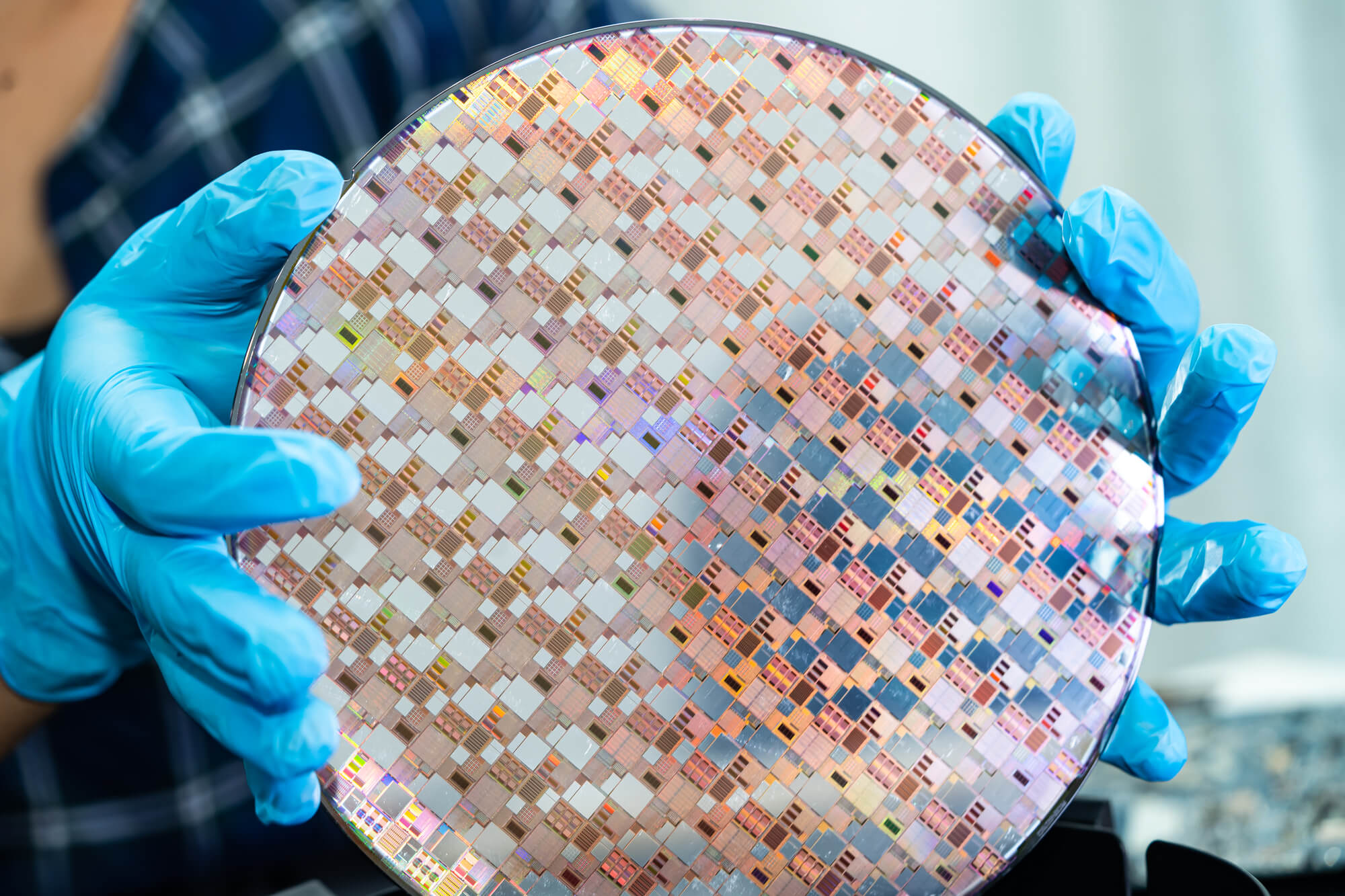
Advances in bendy silicon can potentially change the game for silicon wafer suppliers. Let's explore the future of this phenomenon.
Read More


