.webp)
Stay up-to-date with the latest news and trends in wafer and semiconductor technologies.
*Blogs are for educational and informational purposes ONLY
We prioritize sustainable practices in our silicon manufacturing process through our commitment to environmental responsibility. Learn more about it today!
Read More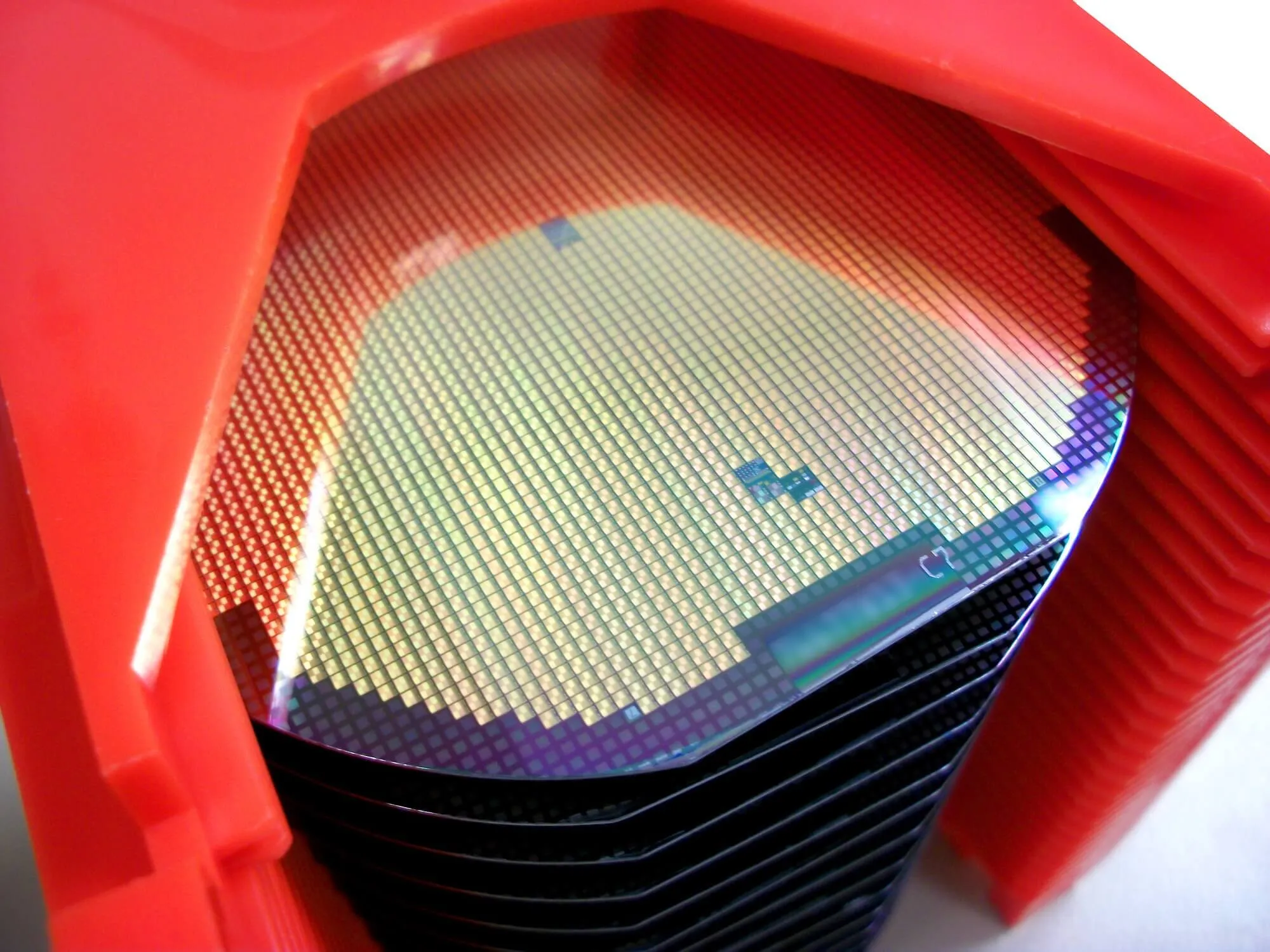
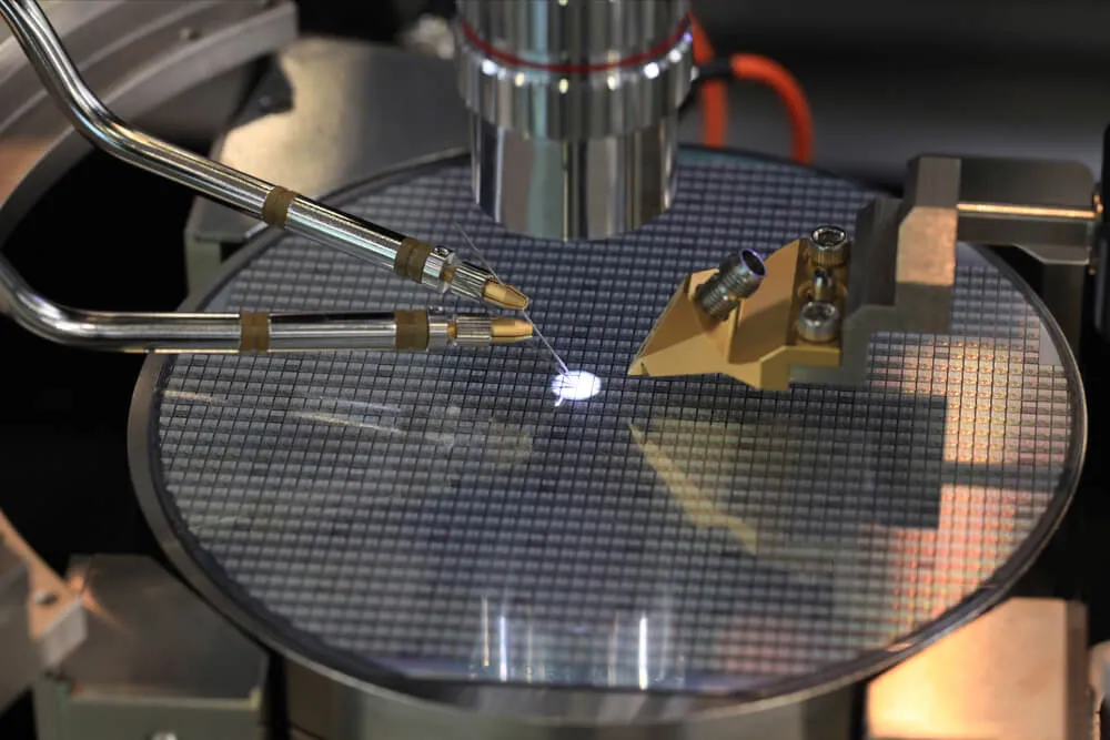
Laser marking in semiconductor wafer manufacturing is crucial for traceability and quality control. Learn about the benefits of laser marking in this industry.
Read More
Thin silicon wafers are essential for advanced sensors and IoT devices. Learn more about the importance of these wafers in the development of cutting-edge technology!
Read More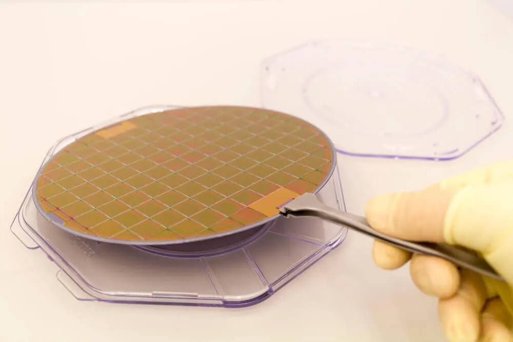
Discover the crucial role germanium wafers play in semiconductor technology and how they are used in electronic devices. Learn more about their applications here.
Read More
Unlock the reality behind InP reclaim wafers and their role in the semiconductor industry. Learn more about the process and benefits of using INP reclaim wafers.
Read More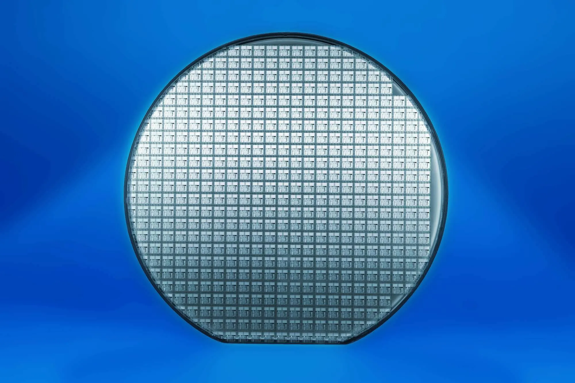
Explore how GaAs reclaim wafers are providing sustainable solutions across industries, offering cost-effective and environmentally friendly options for production processes.
Read More
Discover effective tactics for Silicon Wafer Suppliers to enhance their business and attract more customers. Learn how to stand out in the market and achieve success.
Read More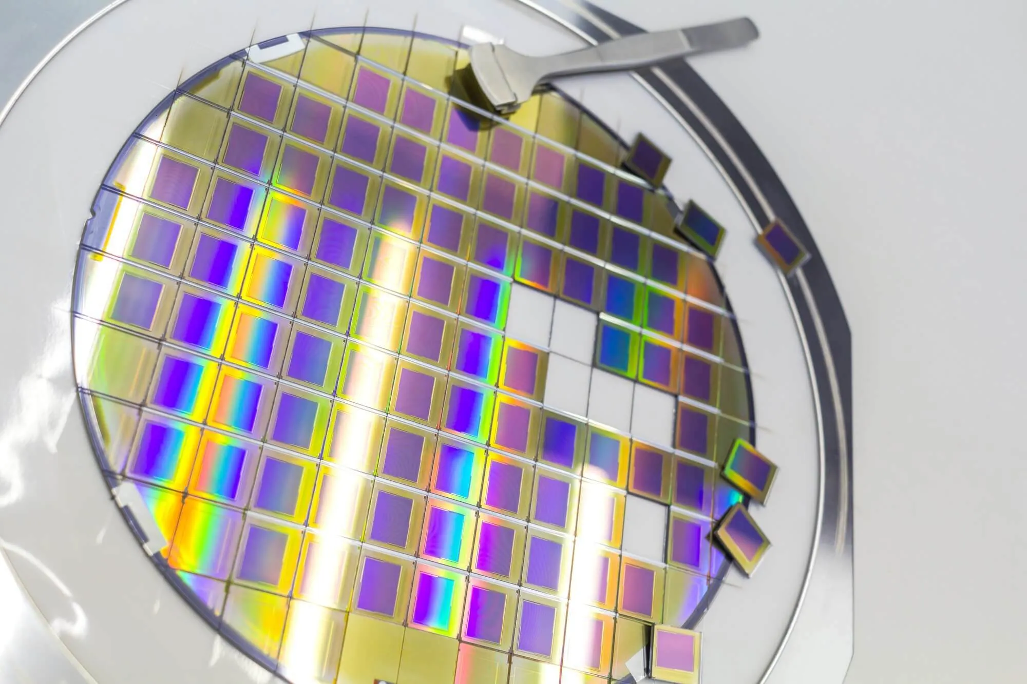
Wafer manufacturing involves the use of nanotechnology to create small, intricate electronic components. Learn more about the benefits of using nanotechnology here.
Read More
Explore the potential of InP wafers for future wireless communication technologies. Learn more about the advancements in this cutting-edge technology.
Read More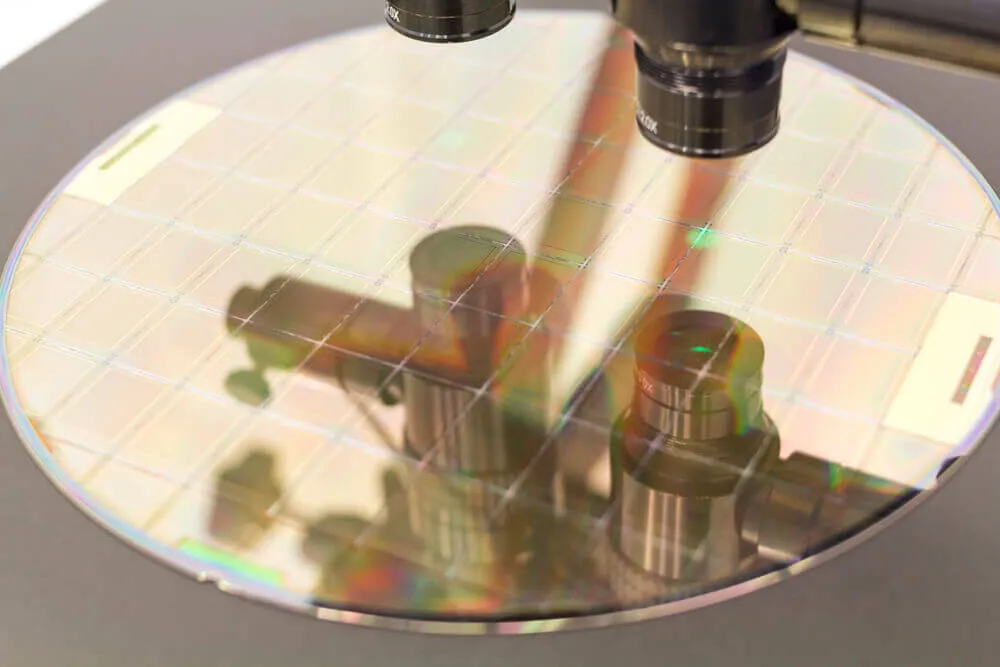
Discover the differences between CZ and FZ wafers and learn more about their properties and uses in the semiconductor industry. Explore today!
Read More