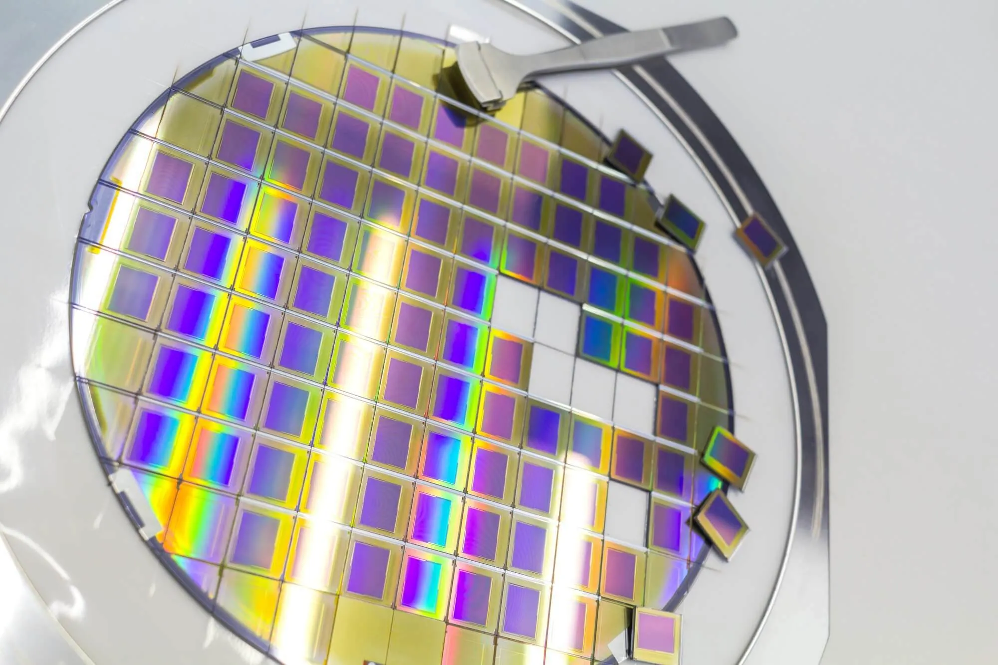
Nanotechnology, with its capability to manipulate materials at the atomic or molecular level, has emerged as a driving force in wafer manufacturing. This article aims to provide an in-depth exploration of the multifaceted applications of nanotechnology in wafer fabrication, elucidating its pivotal role in driving innovation and shaping the future of semiconductor technology.
As we start studying the elaborate landscape of nanotechnology-enabled wafer manufacturing, we will look into the diverse array of nanomaterials, nanopatterning techniques, nanoscale etching and deposition processes, and the revolutionary advancements in nanoelectronics and quantum devices.
Moreover, we will explore additional facets of nanotechnology's impact on wafer manufacturing, including its role in enhancing sustainability, enabling new functionalities, expanding the frontier of materials science, encouraging collaboration and knowledge exchange within the semiconductor industry, and driving advancements in manufacturing automation and process control.
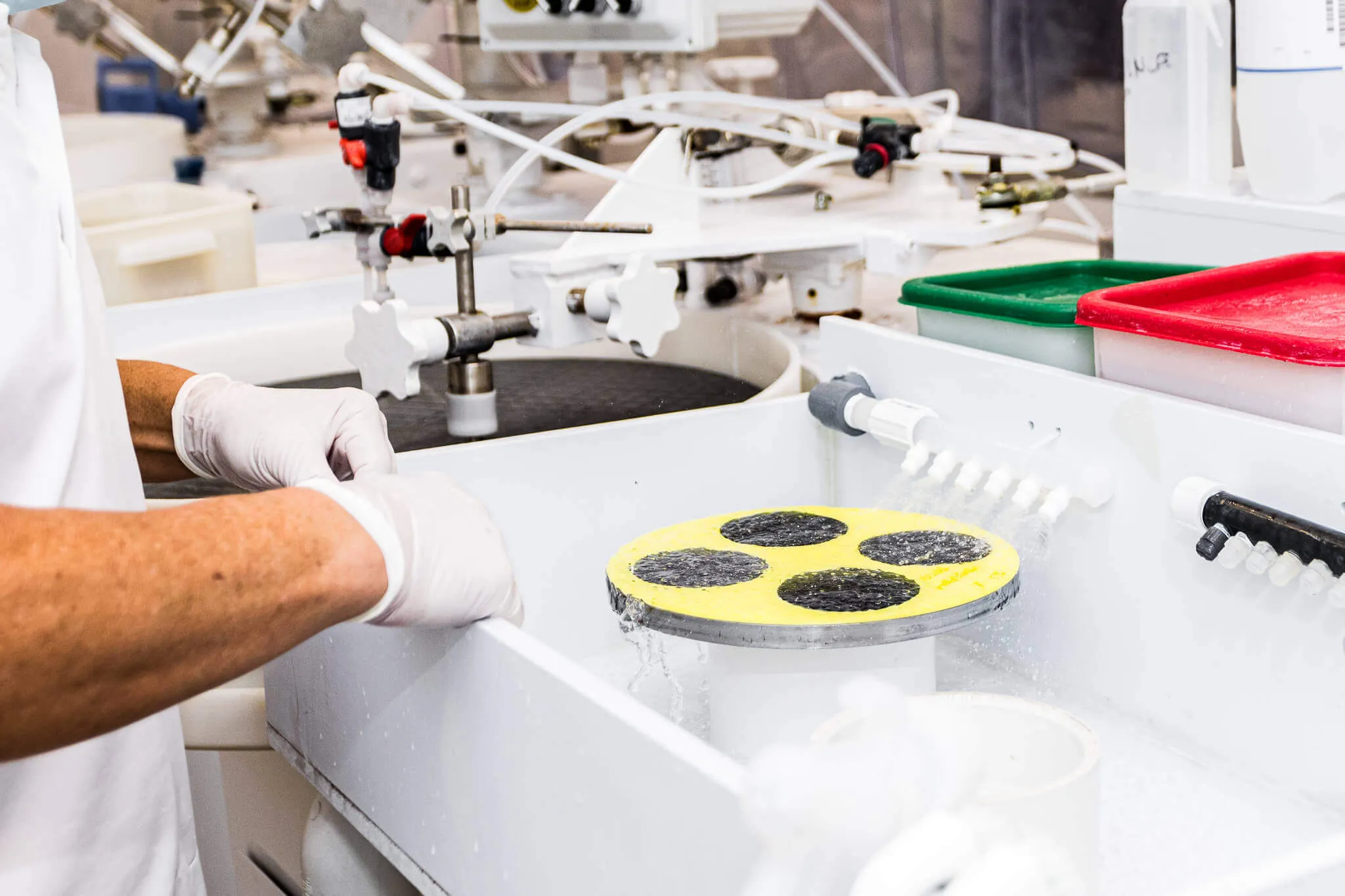
In addition to revolutionizing materials and processes, nanotechnology has also played a significant role in driving advancements in manufacturing automation and process control within the semiconductor industry. Nanotechnology-enabled sensors and monitoring devices offer real-time insights into wafer fabrication processes, enabling proactive maintenance and optimization of equipment performance.
Furthermore, nanomaterial-based coatings and surface treatments enhance the durability and reliability of semiconductor manufacturing equipment, reducing downtime and improving overall productivity. These advancements in manufacturing automation and process control underscore the capability of nanotechnology in streamlining wafer manufacturing processes and warranting the consistent production of high-quality semiconductor devices.
Beyond traditional semiconductor applications, nanotechnology has opened up new possibilities for wafer manufacturing in emerging fields such as nanophotonics and plasmonics. Nanopatterning techniques enable the fabrication of optical and photonic devices with unprecedented precision and functionality. For example, plasmonic nanostructures fabricated using nanolithography techniques exhibit unique optical properties, enabling applications such as enhanced light-matter interactions and sensing.
Photonic crystals created through nanopatterning offer control over the flow of light, paving the way for advanced optical communication and sensing devices. These advancements highlight the versatility of nanotechnology in driving innovation across a diverse range of applications in wafer manufacturing.
Nanotechnology-driven etching and deposition processes not only enable the fabrication of semiconductor devices but also hold promise for applications in emerging fields such as nanoelectromechanical systems (NEMS) and quantum computing. Nanoscale etching techniques can be used to create intricate patterns on nanoscale mechanical and electromechanical devices, enabling the development of advanced NEMS with enhanced performance and functionality.
In the same way, nanomaterial-based thin films deposited using advanced deposition techniques offer unique properties that are critical for the development of qubits and other quantum computing elements. These developments underscore the potential of nanotechnology in enabling the development of next-generation computing and sensing devices with unprecedented capabilities.
In addition to conventional semiconductor materials, nanotechnology has paved the way for the development of novel materials with unique properties tailored for specific applications in wafer manufacturing. For instance, two-dimensional materials such as graphene and transition metal dichalcogenides exhibit exceptional electrical, optical, and mechanical properties, making them promising candidates for next-generation electronic and optoelectronic devices.
Likewise, organic and hybrid organic-inorganic materials offer flexibility, transparency, and low-cost fabrication, opening up new avenues for applications in flexible electronics, organic light-emitting diodes (OLEDs), and organic photovoltaics. These materials, combined with nanotechnology-driven fabrication techniques, hold the potential to revolutionize wafer manufacturing and enable the development of advanced electronic devices with enhanced performance and functionality.
Nanotechnology has also facilitated advancements in materials science, enabling the development of novel nanomaterials with tailored properties for applications in wafer manufacturing. For example, functional nanomaterials such as carbon nanotubes, quantum dots, and perovskite nanocrystals offer unique optical, electrical, and thermal properties, making them promising candidates for applications in sensors, displays, and energy devices.
Similarly, biomimetic nanomaterials inspired by natural systems offer unprecedented control over material properties and functionalities, opening up new possibilities for applications in biotechnology, medicine, and environmental sensing. These advancements highlight the potential of nanotechnology in expanding the frontier of materials science and driving innovation across a diverse range of applications in wafer manufacturing.
Nanotechnology-enabled sensing devices and microelectromechanical systems (MEMS) have also benefited from advancements in wafer manufacturing. Nanomaterial-based sensors offer unparalleled sensitivity, selectivity, and response time, enabling the detection of a wide range of analytes with high accuracy. MEMS devices fabricated using nanotechnology exhibit improved performance characteristics, such as higher sensitivity, lower power consumption, and reduced size, opening up new opportunities for applications in healthcare, environmental monitoring, and industrial sensing.
These developments underscore the capacity of nanotechnology to enable the development of advanced sensing and MEMS devices with enhanced performance and functionality.
While nanotechnology has made significant strides in wafer manufacturing, several challenges remain to be addressed to fully realize its potential. Scalability, cost-effectiveness, and process integration continue to be key areas of focus for researchers and industry stakeholders. Furthermore, the development of sustainable and environmentally friendly nanomaterials and processes is essential to maintain the long-term viability of nanotechnology-enabled wafer manufacturing. Future directions in nanotechnology for wafer manufacturing encompass the development of novel materials, fabrication techniques, and integration strategies to address these challenges and unlock new opportunities for innovation.
Nanotechnology has emerged as a force in wafer manufacturing, unlocking new possibilities and propelling the industry into a future defined by innovation and excellence. From enhancing collaboration and knowledge exchange to enabling new functionalities, expanding the frontier of materials science, promoting collaboration and knowledge exchange within the semiconductor industry, and driving advancements in manufacturing automation and process control, nanotechnology holds the potential to revolutionize the semiconductor industry and shape the future of technology.
As researchers from Wafer World continue to push the boundaries of what is possible, nanotechnology will play an increasingly important role in driving innovation and shaping the future of wafer manufacturing. By harnessing the power of nanotechnology and embracing interdisciplinary collaboration, we can unlock new opportunities and propel the industry into a future defined by innovation, sustainability, and excellence. Contact us to order!


