For silicon wafers to function properly, they need to be nearly perfect. Even after seemingly making it through the entire wafer manufacturing process without any noticeable problems, the wafer can still be useless as a semiconductor. Just the tiniest of issues can cause a problem. In these cases, the wafer will be completely discarded. At Wafer World, our goal is to always provide quality silicon wafers to our customers. This means that we always fully test our wafers at the end of the manufacturing process. We strive to ensure that you will be receiving a high-quality product. To properly showcase the extra care we take from the beginning to when they are in your possession, let’s take a look at what we do to ensure you have a satisfactory silicon wafer.
Before we dive into the testing phase of the manufacturing process, what are the steps that need to be taken first to create the silicon wafer? We won’t get into every detail here, but let’s look at a brief overview to get a better idea.
Wafer sorting is just another way of saying wafer testing. It even has some other names as well, which include electronic die sorting and circuit probing. The goal of the test is simple – test a silicon die in wafer form to determine if it’s functional or not. If it’s a non-functional die, it will not be packaged. Every wafer and silicon die are tested so that our customers can be assured they will have a fully functional semiconductor when they are ready to use it. It is a great assistance in the manufacturing process as well, because if one is found to be non-effective, it won’t go through the final steps. This means we avoid extra expenses, also keeping the cost of wafers down.
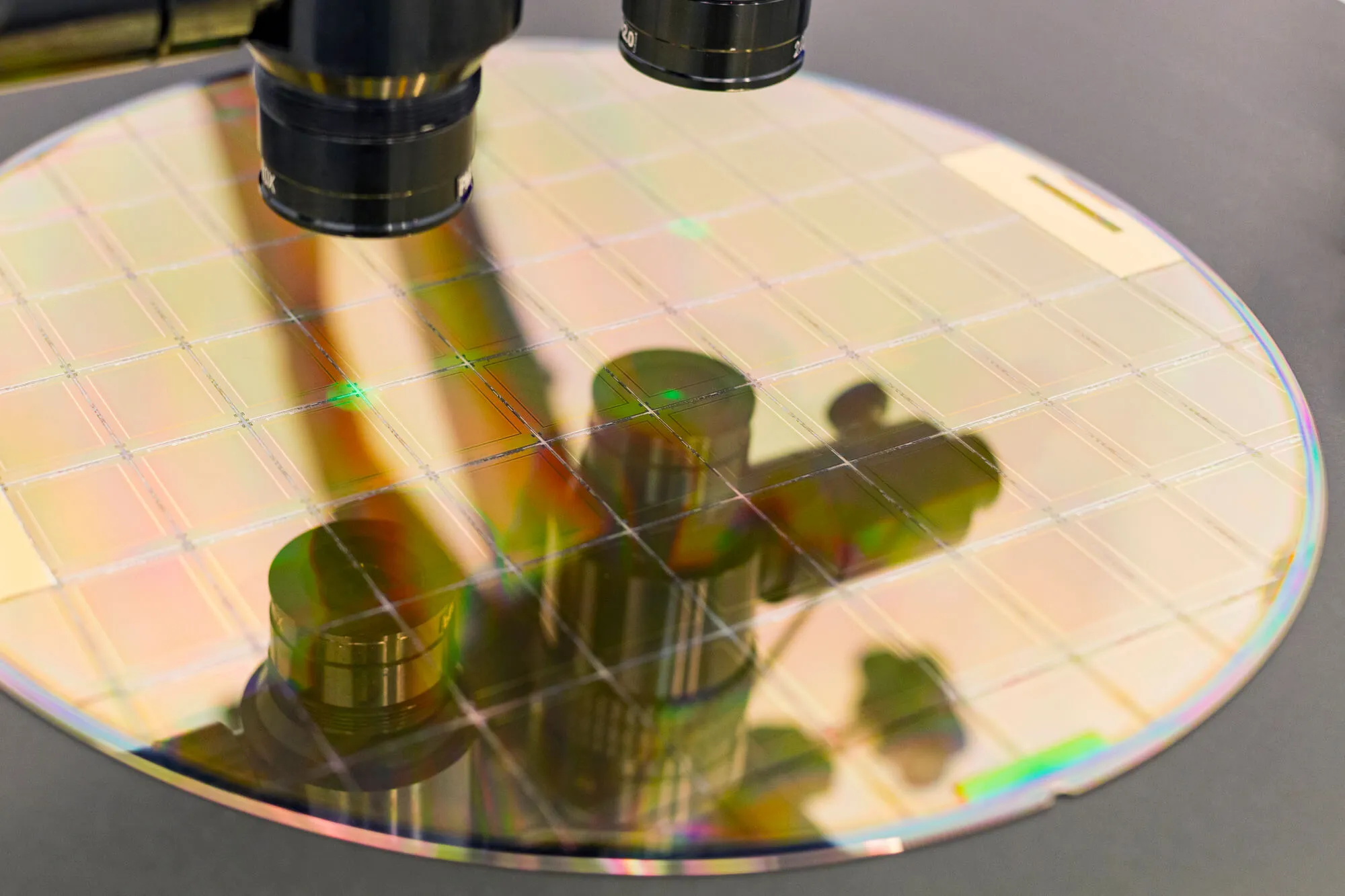
There’s a lot of tiny pieces that sit on a finished silicon wafer. Unfortunately, this makes testing with the naked eye practically impossible. So, we complete testing with the use of a special machine that uses patterns to detect any possible defects with the integrated circuits. Then, they continue on to be packaged. So, what kind of machine is used to test the wafers during this process? That job goes to the wafer prober. An automated machine solely used to test integrated circuits in the manufacturing process. To use the machine for testing, the silicon wafer is vacuum sealed on a wafer chuck, which is a round device that is meant to be a little bit bigger than the wafer. In most cases, this means that it will have a diameter somewhere between 50 mm and 300 mm. They are most commonly made of aluminum with a nickel plating, but they can also be made of steel.

While the wafer is mounted on the wafer chuck, a probe card, which is a set of microscopic contacts, is held as the wafer is properly positioned for electrical contact. This is when the needles on the prober touch the contact pads of the wafer. Electricity will easily be conducted if the wafer is functional as a semiconductor. On the chance that the electricity does not flow as required, the wafer is considered to be defective and discarded. After successfully completing this testing stage, the prober will then transfer the wafer to test another line. When the wafer is complete, it is vital it has the lowest amount of human interaction possible. There are many opportunities to damage the wafer due to their high sensitivity. A damaged wafer is a useless wafer. Therefore, having an automated machine allows the process to move smoothly with a low risk of accidents.
Substrate mapping, which is also more easily known as wafer mapping, is a process of visually identifying semiconductor performance through color-coding. Each color represents a potential issue with the wafer. This allows the production process to be analyzed as to why a deviation could be occurring. This is crucial in figuring out how to improve the manufacturing process.
Once everything is completed and the wafers are properly packaged, it’s time to complete one more test. You might be questioning why another test needs to be completed. We have already discovered that the wafers are functional semiconductors, right? This test, which isn’t much different than the original testing process, is very useful for detecting issues with the assembly process. Some small but important things may be caught, like missing wire bonds or bumps. It’s a step that doesn’t necessarily need to be taken, but we are always looking to provide top quality wafers!

If you’re in need of silicon wafers, we know that finding a high-quality product is extremely important to you. That’s why we always do our best to provide wafers that are expertly crafted. No shortcuts. No cutting corners. Your satisfaction with our product is our top priority and we strive to deliver every time. If you have any questions about our silicon wafers or you’d like to make a purchase, contact us today for inquiries.


