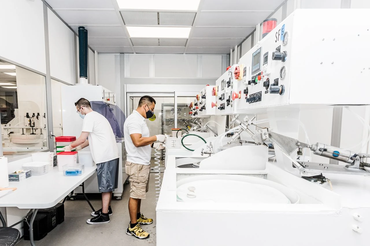
A germanium wafer remains an important material in advanced electronics, infrared systems, and semiconductor research. Although silicon dominates many manufacturing applications, germanium continues to offer valuable electrical and optical advantages that support specialized technologies. Researchers, engineers, and manufacturers often rely on germanium-based materials when performance requirements demand high conductivity, infrared transparency, or compatibility with precision fabrication processes.
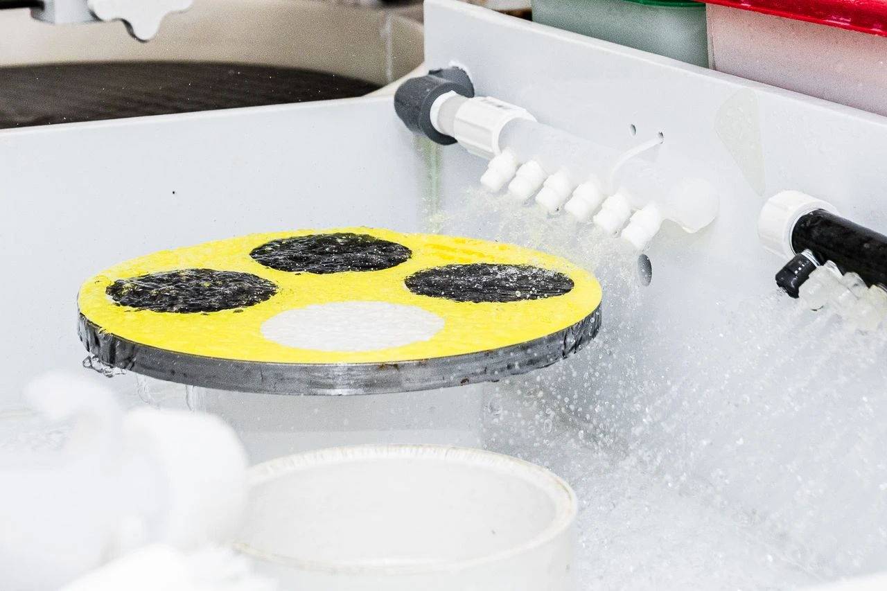
Germanium is a semiconductor element known for its strong infrared transmission and high electron mobility. These characteristics make it useful in applications where speed, signal sensitivity, and optical efficiency are critical. While the semiconductor industry primarily uses silicon for mainstream electronics, germanium continues to play an important role in high-performance and research-driven environments.
A germanium wafer is created by slicing a purified germanium crystal into thin, highly controlled discs. Manufacturers process these wafers to meet strict standards involving thickness, crystal orientation, surface quality, and resistivity. Depending on the intended use, wafers may also undergo polishing, etching, or doping procedures to achieve specific material properties.
Because of its unique properties, germanium remains relevant in industries that require advanced sensing, optical precision, and specialized semiconductor capabilities.
Germanium is widely recognized for its infrared transparency. This property makes it highly suitable for thermal imaging systems, infrared lenses, spectroscopy equipment, and night vision technologies. Defense contractors, aerospace manufacturers, and industrial inspection companies often depend on germanium-based optical components to support imaging accuracy in low-visibility environments.
Infrared applications require materials that maintain optical performance under demanding conditions. Germanium provides reliable infrared transmission, making it a preferred choice for many advanced optical systems.
Researchers continue exploring germanium for next-generation semiconductor technologies. The material’s electron mobility can enable faster signal processing than traditional semiconductor materials in certain applications. Laboratories and research facilities use germanium substrates to study transistor performance, integrated circuits, and advanced chip structures.
As semiconductor demands evolve, germanium continues to attract interest for its potential to improve electronic speed and energy efficiency.
Germanium substrates are commonly used in multi-junction solar cells designed for aerospace and satellite systems. These solar technologies prioritize high efficiency and long-term reliability, particularly in environments where energy generation is critical.
Because germanium is compatible with complex photovoltaic structures, it remains valuable for specialized energy applications that require advanced material performance.
Germanium also contributes to sensors and precision electronics. Its electrical characteristics help support devices that rely on accurate signal processing, thermal responsiveness, and conductivity. Specialized industrial equipment and laboratory instrumentation often incorporate germanium-based components where precision matters most.
Choosing the right wafer involves evaluating multiple technical factors. Understanding these specifications can help buyers avoid compatibility problems and improve long-term project outcomes.
Crystal orientation refers to the alignment of atoms within the wafer structure. Common orientations include (100), (111), and (110). Different applications require specific orientations depending on fabrication methods and performance goals.
Orientation affects etching behavior, surface structure, and device manufacturing processes. Selecting the appropriate orientation ensures compatibility with downstream processing requirements.
Wafer diameter influences manufacturing capacity and equipment compatibility. Smaller wafers are often suitable for laboratory research and prototyping, while larger diameters support commercial-scale production.
Buyers should confirm that wafer sizing aligns with the fabrication equipment and project objectives before placing orders.
Thickness plays a significant role in mechanical stability and processing reliability. Thin wafers may support advanced device structures but can also require extra care during handling and transportation.
Thicker wafers generally offer greater durability and lower breakage risks. Determining the correct thickness depends on processing conditions, device requirements, and operational demands.
Surface quality is essential for semiconductor fabrication and optical performance. Manufacturers may provide polished, double-sided, or etched finishes depending on application needs.
Highly polished surfaces help minimize defects and support precision manufacturing environments. In optical applications, smooth surfaces can improve performance consistency and reduce contamination concerns.
Germanium wafers may be intrinsic or intentionally doped to achieve targeted electrical behavior. Resistivity requirements vary based on device function and processing goals.
Understanding conductivity needs before ordering can help ensure the material performs properly during fabrication and operation. Buyers should review resistivity tolerances carefully to maintain consistency across projects.
Material quality directly affects wafer reliability and manufacturing performance. Buyers should evaluate supplier inspection standards and quality assurance procedures before committing to production orders.
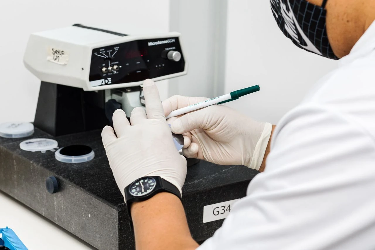
Even minor imperfections can impact semiconductor processing or optical efficiency. Reputable manufacturers typically perform detailed inspections to verify wafer consistency and dimensional accuracy.
Inspection procedures often include:
Maintaining strict quality standards helps improve repeatability in both research and manufacturing environments.
Semiconductor materials require controlled handling conditions to maintain cleanliness and structural integrity. Improper storage or handling can introduce contamination, scratches, or mechanical damage, reducing usability.
Operators should use approved wafer-handling tools and clean gloves when working with semiconductor materials. Controlled environments also help reduce airborne particles that could affect sensitive wafer surfaces.
Recommended storage practices include:
Careful handling procedures can extend material lifespan and help maintain processing reliability throughout fabrication stages.

Not every wafer is designed for the same level of performance or manufacturing scale. Buyers should understand the difference between research-grade and production-grade materials before making purchasing decisions.
Research-grade wafers are commonly used for laboratory experiments, educational settings, and prototype development. These materials may offer greater flexibility for testing and smaller-scale projects.
Production-grade materials typically meet the tighter tolerances and consistency requirements needed for commercial manufacturing. Industries producing advanced electronics, optical systems, and semiconductor devices often depend on production-grade standards to maintain scalability and performance reliability.
Selecting the correct grade can help balance cost considerations with technical requirements.
Germanium remains a specialized semiconductor material, making supplier reliability an important consideration. Buyers involved in long-term manufacturing or recurring research projects should evaluate inventory stability, technical support capabilities, and production consistency.
Lead times may vary depending on wafer specifications and market demand. Building strong supplier relationships can help reduce delays and improve procurement planning over time.
It is also beneficial to communicate detailed specifications clearly before ordering. Alignment between buyers and suppliers can minimize production issues and support more predictable manufacturing outcomes.
Selecting the right germanium wafer supplier involves more than simply reviewing specifications. Material quality, technical consistency, and supplier expertise all contribute to successful research and manufacturing outcomes. Whether supporting infrared optics, semiconductor development, or advanced electronics, choosing reliable wafer solutions can improve operational efficiency and reduce long-term production challenges. At Wafer World, we continue supporting researchers, engineers, and manufacturers with germanium wafer materials designed to meet evolving industry requirements and precision-focused applications.
Contact us today for your wafer needs.




