
Germanium wafers, which had previously been overlooked in favor of silicon counterparts, have acquired substantial popularity in many applications. Wafer World delves into the world of germanium wafers, looking at their qualities, applications, manufacturing method, and future possibilities. Join us as we discover this exceptional semiconductor material's hidden potential.
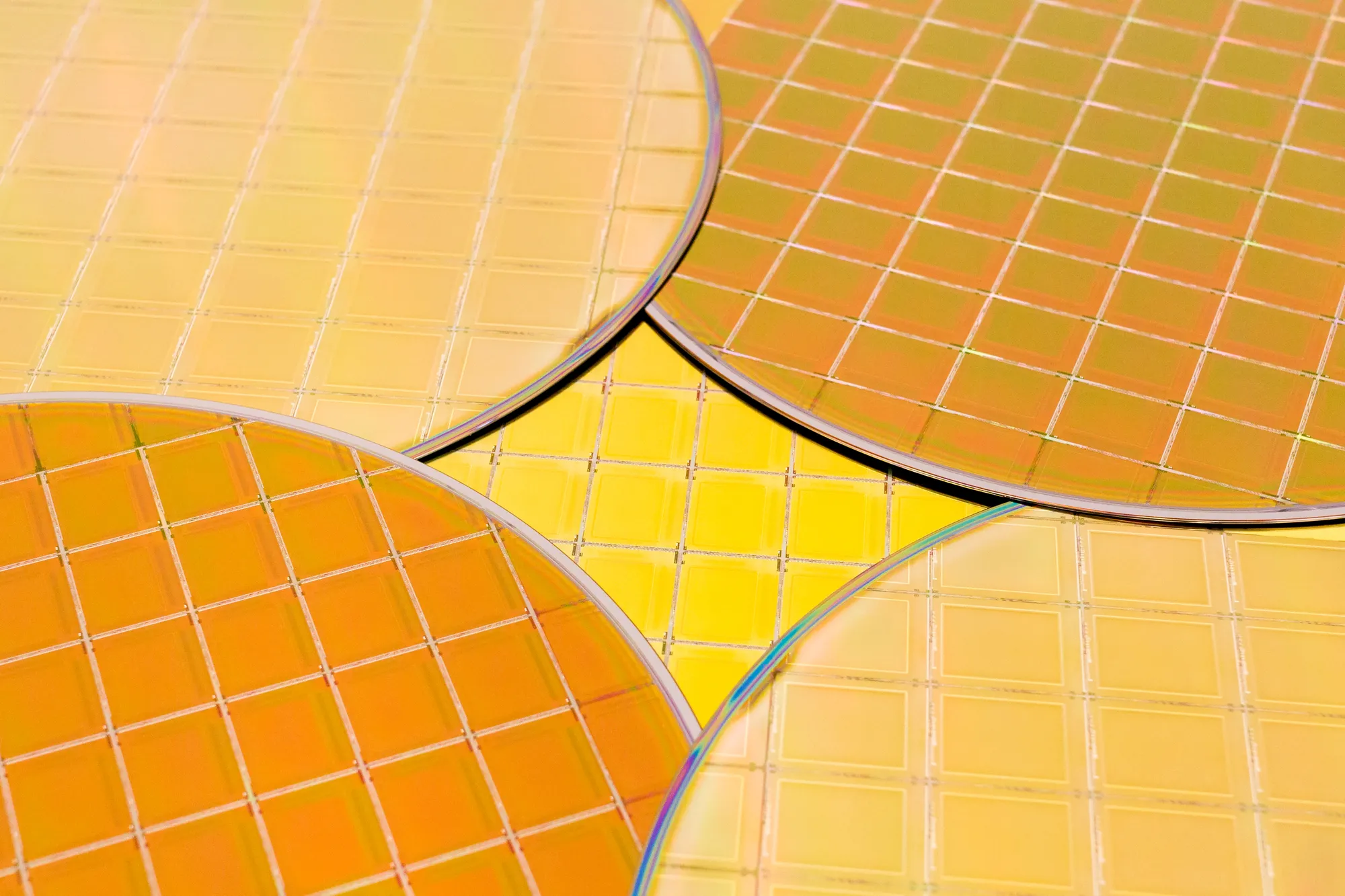
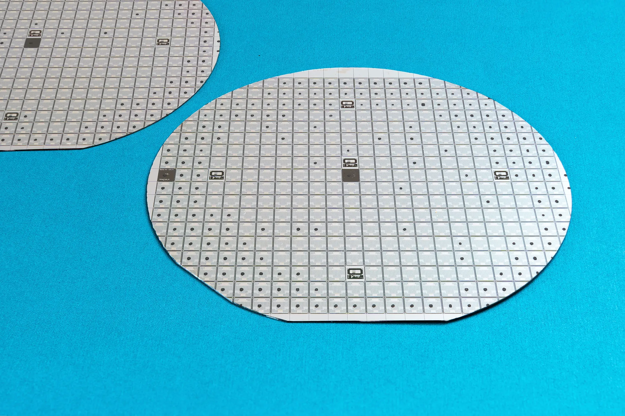
Germanium (Ge) wafers are thin slices of single-crystal germanium, a metalloid element in the periodic table's carbon group. Although silicon wafers dominate the semiconductor industry, germanium wafers have distinct features that make them highly attractive in certain applications.
They have strong thermal conductivity, excellent electrical conductivity, and an inherent capacity to absorb infrared light. These characteristics make germanium wafers indispensable in various industries, including electronics, optics, photovoltaics, and others.
Germanium wafers have various distinguishing characteristics that set them apart from other materials. They have better charge carrier mobility than silicon, making them suited for high-frequency applications. Germanium wafers have a lower bandgap, which allows them to absorb and emit infrared light more efficiently.
Furthermore, its thermal conductivity enables efficient heat dispersion. Because of these characteristics and their compatibility with existing silicon-based technologies, germanium wafers are a prospective choice for various cutting-edge applications.
Germanium wafers are used in a range of industries. They are utilized in high-speed transistors, diodes, and integrated circuits in the realm of electronics, where they outperform silicon. They are used in infrared optics, night vision devices, and thermal imaging systems due to their capacity to absorb infrared light.
Furthermore, germanium wafers are important in photovoltaics because they are the foundation for high-efficiency solar cells. They are also used in fiber optics as a vital material for carrying signals across vast distances.
Due to their excellent characteristics and numerous uses, germanium wafers have developed as a significant semiconductor material. As technology advances, their importance is projected to rise even more. Germanium wafers have carved out their position in the ever-changing world of sophisticated materials, whether in electronics, optics, or renewable energy.
Contact us at Wafer World for more details!


