
At first glance, GaAs reclaimed wafers and GaAs test wafers may appear to be similar—both serve non-device or test functions in semiconductor manufacturing. However, their origin, surface quality, and intended use vary greatly.
Knowing the difference is crucial for engineers seeking to strike a balance between performance, cost, and repeatability in their fabrication processes.
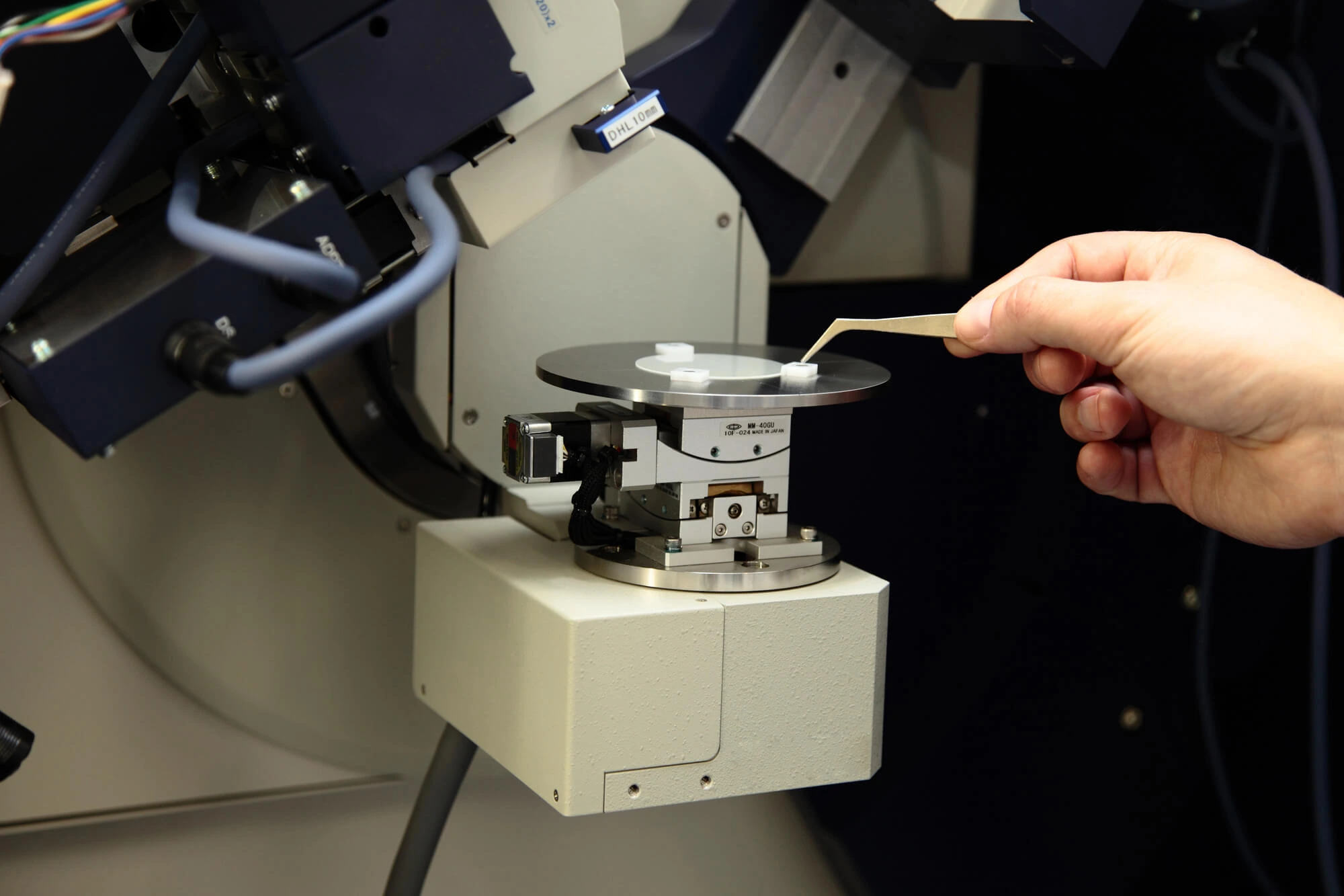
GaAs reclaimed wafers are previously used gallium arsenide substrates that have been chemically and mechanically restored to nearly new condition.
Stripping, polishing, and surface characterization processes are used to restore the flatness, cleanliness, and structural integrity of these wafers in preparation for subsequent testing or deposition steps.
In contrast, GaAs test wafers are typically new, virgin wafers designed specifically for process qualification, calibration, or research applications. They have the same crystal structure and electrical properties as production-grade GaAs wafers. Still, they are used to test process parameters, deposition uniformity, and photolithography accuracy before proceeding to the active device layers.
Because test wafers are new, they provide a perfectly consistent baseline for sensitive applications where surface uniformity and doping levels must match those of production devices.

In short: all reclaimed wafers can serve as test wafers, but not all test wafers are reclaimed. Your choice depends on how critical surface uniformity, doping precision, and contamination control are to your process.
Whether you’re running R&D tests or qualifying a new production tool, selecting the right GaAs wafer type has a significant impact on both performance and cost. If you’re still in doubt about what will work best for you, Wafer World can help. Contact us today to discover how reclaim wafers can optimize your workflow and reduce expenses—without sacrificing quality.


