December 8, 2023
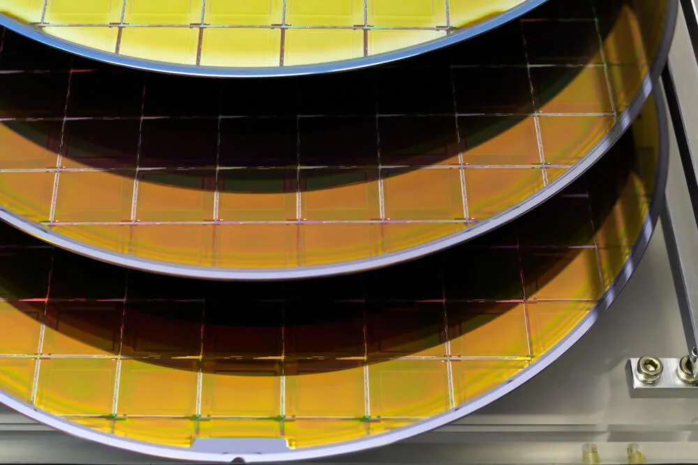
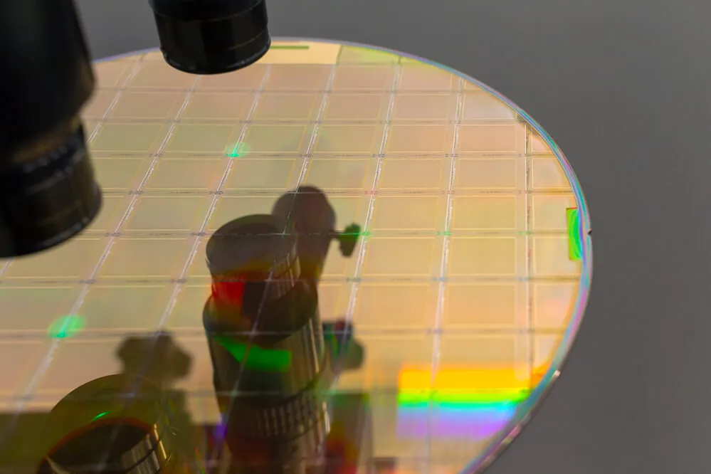
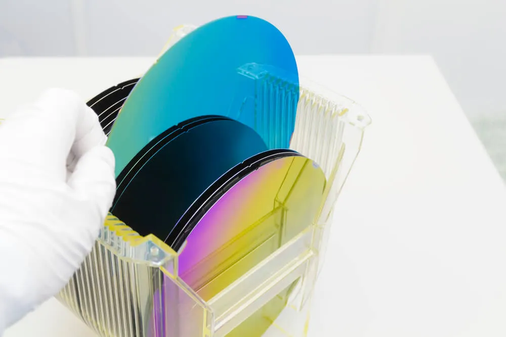
Shop NowIn the fast-paced world of technology, silicon wafers have become synonymous with the heart of electronic devices, forming the backbone of semiconductor manufacturing. However, their utility extends far beyond the realms of traditional electronics.
This blog aims to shed light on the diverse applications of silicon wafers, exploring their pivotal role in non-traditional fields such as solar energy, MEMS (micro-electro-mechanical systems) devices, and other cutting-edge technologies reshaping our future.
One of the most transformative applications of silicon wafers lies in the realm of renewable energy, particularly solar power. Silicon wafers are the building blocks of solar cells, devices that convert sunlight into electricity through the photovoltaic effect.
With its excellent semiconducting properties, silicon is a natural choice for solar cell manufacturing. Monocrystalline and polycrystalline silicon wafers are the foundation for solar panels, capturing sunlight and generating clean energy. The process involves doping the silicon with specific materials to create positive and negative charges, facilitating the flow of electricity.
As the demand for sustainable energy solutions continues to rise, silicon wafers are pivotal in expanding solar technologies. Ongoing research focuses on improving the efficiency of solar cells and exploring novel materials and manufacturing techniques to make solar energy more accessible and cost-effective.
Micro-electro-mechanical systems, or MEMS, represent another frontier where silicon wafers showcase their versatility. MEMS devices are miniature systems that integrate mechanical and electrical components on a tiny silicon chip. These devices find applications in an array of fields, from healthcare to consumer electronics.
Silicon wafers serve as the canvas upon which intricate MEMS structures are etched. The manufacturing process involves using specialized lithography techniques to create micron-sized structures, such as sensors, actuators, and valves. MEMS devices have found their way into everyday gadgets like smartphones, where they power accelerometers and gyroscopes, enabling features like screen rotation and motion sensing.
In the medical field, silicon-based MEMS devices are revolutionizing healthcare by providing precise and compact tools for diagnostics and treatment. Microsensors embedded in these devices can monitor various physiological parameters, offering real-time data for personalized healthcare solutions.
The journey of silicon wafers doesn't stop with solar cells and MEMS devices. As technology evolves, so does the range of applications for these versatile substrates.
Silicon wafers are crucial in the race to achieve quantum computing supremacy. Quantum computers, which harness the principles of quantum mechanics, have the potential to revolutionize computation by solving complex problems at speeds unimaginable with classical computers.
With their established manufacturing processes and compatibility with existing semiconductor technologies, silicon wafers are at the forefront of quantum computing research. Quantum dots, which can be integrated into silicon wafers, are being explored as potential qubits, the fundamental units of quantum information. The marriage of silicon wafers and quantum computing promises to unlock unprecedented computational power, with implications for fields such as cryptography, optimization, and material science.
The era of rigid electronic devices gradually gives way to flexible and bendable electronics, and silicon wafers are part of this transformative shift. Researchers and engineers are developing electronics that can conform to various shapes and surfaces by leveraging the flexibility of thin silicon wafers.
Flexible displays, wearable electronics, and rollable solar panels are just a few examples of the exciting possibilities that flexible electronics offer. When thinned down to the nanoscale, silicon wafers retain their semiconductor properties while gaining the flexibility required for these innovative applications. This convergence of traditional silicon technology with flexibility opens new avenues for design and functionality in electronic devices.
The intersection of silicon wafers and biotechnology yields groundbreaking innovations in diagnostics and medical research. Lab-on-a-chip devices, often fabricated on silicon wafers, enable integrating multiple laboratory functions onto a single chip. This miniaturization of diagnostic tools enhances efficiency, reduces costs, and accelerates the pace of medical testing.
Microfluidic devices, etched onto silicon wafers, facilitate the precise control of tiny amounts of fluids, allowing for rapid and accurate diagnostic assays. These devices have applications ranging from point-of-care diagnostics to DNA analysis, contributing to advancements in personalized medicine and disease detection.
The demands of space exploration require robust and reliable technology, and silicon wafers are at the forefront of enabling cosmic discoveries. Silicon-based sensors and imaging devices are integral to space probes, telescopes, and satellites.
In space telescopes, silicon wafers are used to construct charge-coupled devices (CCDs) that capture and process light, allowing astronomers to observe distant galaxies and celestial phenomena. The reliability and stability of silicon make it an ideal material for withstanding the harsh conditions of space, contributing to the success of various space missions.
As the world grapples with environmental challenges, silicon wafers are finding applications in monitoring and mitigating the impact of human activities on the planet. Silicon-based sensors are deployed in environmental monitoring devices to measure air and water quality, soil conditions, and pollutant levels.
These sensors, often fabricated on silicon wafers, provide real-time data crucial for assessing environmental health and implementing measures to address pollution and climate change. The precision and reliability of silicon-based environmental sensors contribute to our understanding of ecological systems and support efforts to create a more sustainable future.
The applications of silicon wafers extend far beyond their traditional role in electronics. From harnessing solar energy to powering miniature devices in the world of MEMS and pushing the boundaries of emerging technologies like quantum computing and flexible electronics, silicon wafers are proving to be a linchpin in the evolution of our technological landscape.
As Wafer World continues to explore and push the boundaries of what is possible, silicon wafers will undoubtedly play a pivotal role in shaping the future of diverse industries. Whether it's capturing sunlight to create clean energy or enabling the development of quantum computers with unimaginable processing power, the journey of silicon wafers beyond electronics is a testament to the adaptability and resilience of this foundational material. Call us to order!


