
In today's technologically advanced world, the ubiquitous presence of electronic devices has become an integral part of our daily lives. Behind the scenes of these devices lies a remarkable component known as the silicon wafer. Often overlooked by the average consumer, silicon wafers play a crucial role in powering the electronics that have transformed how we communicate, work, and entertain ourselves.
In this blog post, we will delve into the fascinating world of silicon wafer processing, exploring their composition, manufacturing process, and the myriad of applications that rely on their exceptional properties.
https://www.waferworld.com/post/from-sand-to-superpowers-the-magic-of-silicon-wafer
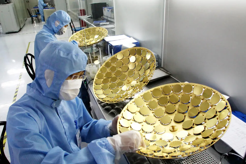
A silicon wafer, simply put, is a thin disc made from crystalline silicon – a material derived from sand, one of the Earth's most abundant resources. The manufacturing process involves several intricate steps, including purification, crystal growth, slicing, polishing, and doping. The result is a flat, round wafer with an incredibly smooth and uniform surface.
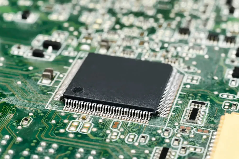
At the heart of our digital age, silicon wafers are indispensable in shaping the integrated circuits that underpin virtually every electronic device we rely on. These microscopic wonders result from intricate processes involving layering, etching, and doping various regions of the silicon wafer to create transistors, resistors, and capacitors. Transistors, in particular, act as the building blocks of logic gates, allowing for complex computations and data processing.
The continuous advancement of lithography techniques has enabled the production of ever-smaller transistors, leading to the exponential growth in computing power described by Moore's Law. Thus, silicon wafers are not just materials; they are the bedrock of the digital revolution, enabling the creation of more powerful, efficient, and compact devices with each passing year.
Photovoltaic Cells Beyond powering our gadgets, silicon wafers have also sparked a renewable energy revolution through their role in photovoltaic cells. These cells, also known as solar cells, utilize the photoelectric effect to convert sunlight into electricity. The silicon wafers within these cells absorb photons from the sun, liberating electrons and generating an electric current.
As a result, solar panels have become emblematic of sustainable energy generation, finding their way onto rooftops, remote installations, and even spacecraft. The use of silicon wafers in photovoltaic cells underscores their versatility – from enabling our digital world to harnessing the power of the sun – making them a cornerstone of both technological and ecological progress.
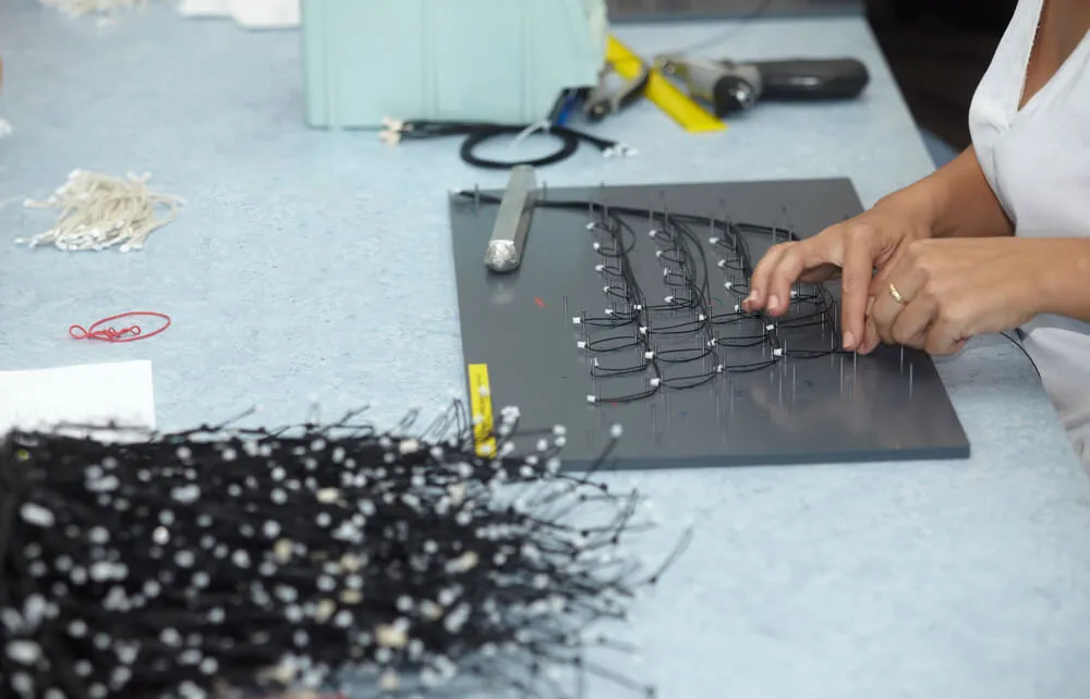
Silicon wafers extend their influence into the realm of micro-scale mechanical systems and sensors, opening doors to innovations in various industries. Micro-electro-mechanical systems (MEMS) leverage the precision of silicon wafers to craft tiny, intricate mechanical structures and sensors. These components have transformed our daily lives, from the inertial sensors that enable smartphone screen rotation to the pressure sensors that monitor tire pressure in vehicles.
MEMS devices often involve moving parts on a minuscule scale, showcasing the astounding precision achievable with silicon wafer fabrication. These systems continue to redefine industries as diverse as healthcare, automotive, and consumer electronics, exemplifying the remarkable intersection of silicon technology and the tangible world around us.
In the realm of optoelectronics, silicon wafers demonstrate their adaptability by enabling the creation of devices that seamlessly merge light and electricity. Light-emitting diodes (LEDs) and laser diodes, essential to modern lighting, displays, and communication systems, are fashioned on silicon wafers. These wafers undergo intricate processes to engineer the precise structures necessary for manipulating photons and generating light emissions.
The marriage of silicon's electronic prowess with its newfound capacity to manipulate light has resulted in transformative advancements, from energy-efficient lighting solutions to high-speed fiber-optic communication networks. This convergence of traditional electronics and photonics illustrates how silicon wafers continually push the boundaries of what's achievable in the world of technology.
The medical field, too, has been profoundly impacted by optoelectronics. Silicon wafer-based sensors are integrated into various medical devices, facilitating non-invasive diagnostic procedures. Optical sensors can measure factors such as blood oxygen levels and glucose concentrations, offering valuable insights into a patient's health status. Additionally, optoelectronics plays a significant role in imaging technologies like optical coherence tomography (OCT), which provides high-resolution images for diagnosing eye conditions and other medical issues.
Silicon wafers extend their influence into the realm of power electronics, where their unique properties are harnessed to manage and control high levels of electrical power. Silicon carbide (SiC) wafers, a variant of traditional silicon wafers, have garnered attention for their exceptional characteristics, including higher thermal conductivity and greater energy efficiency.
SiC wafers are utilized to craft power devices capable of handling intense voltages and frequencies, making them ideal for applications such as electric vehicles, industrial motor drives, and renewable energy systems. As our society seeks more efficient and sustainable ways to harness and distribute power, silicon wafers continue to evolve and diversify their role, shaping the landscape of modern energy management.
As the demand for energy-efficient solutions and sustainable power sources continues to rise, the role of silicon wafers in power electronics becomes increasingly crucial. SiC-based power devices not only contribute to reduced energy consumption and lower greenhouse gas emissions but also pave the way for technological advancements in diverse sectors, from transportation to industrial automation.
From the intricate circuitry of our smartphones to the sprawling solar farms harnessing sunlight, silicon wafers are at the forefront of modern technological innovation. These unassuming discs of purified sand have transformed the way we interact with the world and power our societies.
As technology continues to advance, silicon wafers from Wafer World will likely continue to evolve, enabling new possibilities and pushing the boundaries of what we can achieve in the realm of electronics and beyond.
When you turn to us for your wafer needs, you can expect nothing but the highest quality wafers made with extreme attention to detail. Our team always strives for the best product possible, so you know what you’re getting every time you make a purchase. Ready to see the Wafer World difference? Order now or give us a call to learn more about our products.


