Ultra-thin silicon wafers have become increasingly significant in the semiconductor industry, enabling the development of advanced electronic devices. However, their production poses unique challenges that require innovative solutions. Delve into the challenges faced in manufacturing ultra-thin silicon wafers and explore the cutting-edge innovations and techniques that address these challenges.
Since thin silicon wafers are used in electronics and micromechanical devices, they play a significant role in the semiconductor industry. While this device has numerous uses, the question remains about the challenges and innovations in manufacturing thin silicon wafers.
Thin wafers, or ultra-thin wafers, refer to semiconductor wafers with significantly reduced thickness compared to standard wafers. These wafers are typically made of silicon, gallium arsenide, or other semiconductor materials.
The term "thin" is relative and can vary depending on the context and application. In general, thin wafers are characterized by their reduced thickness, often ranging from a few micrometers to a fraction of a millimeter. These wafers can be as thin as a few microns (µm) or even sub-micron levels (nanometers), depending on the application's specific requirements.
Thin wafers offer several advantages in various industries, including microelectronics, optoelectronics, and sensors. Their reduced thickness provides enhanced flexibility, improved thermal dissipation, increased integration density, and improved device performance. The thinness of these wafers enables the fabrication of more compact and lightweight devices, making them well-suited for applications where size and weight constraints are critical.
Manufacturing thin wafers involves specialized processes, including wafer-thinning techniques such as grinding, etching, and polishing. These processes reduce the thickness of the wafers while maintaining their structural integrity and surface quality. Thinning techniques must be carefully controlled to ensure precise thickness uniformity across the entire wafer surface.
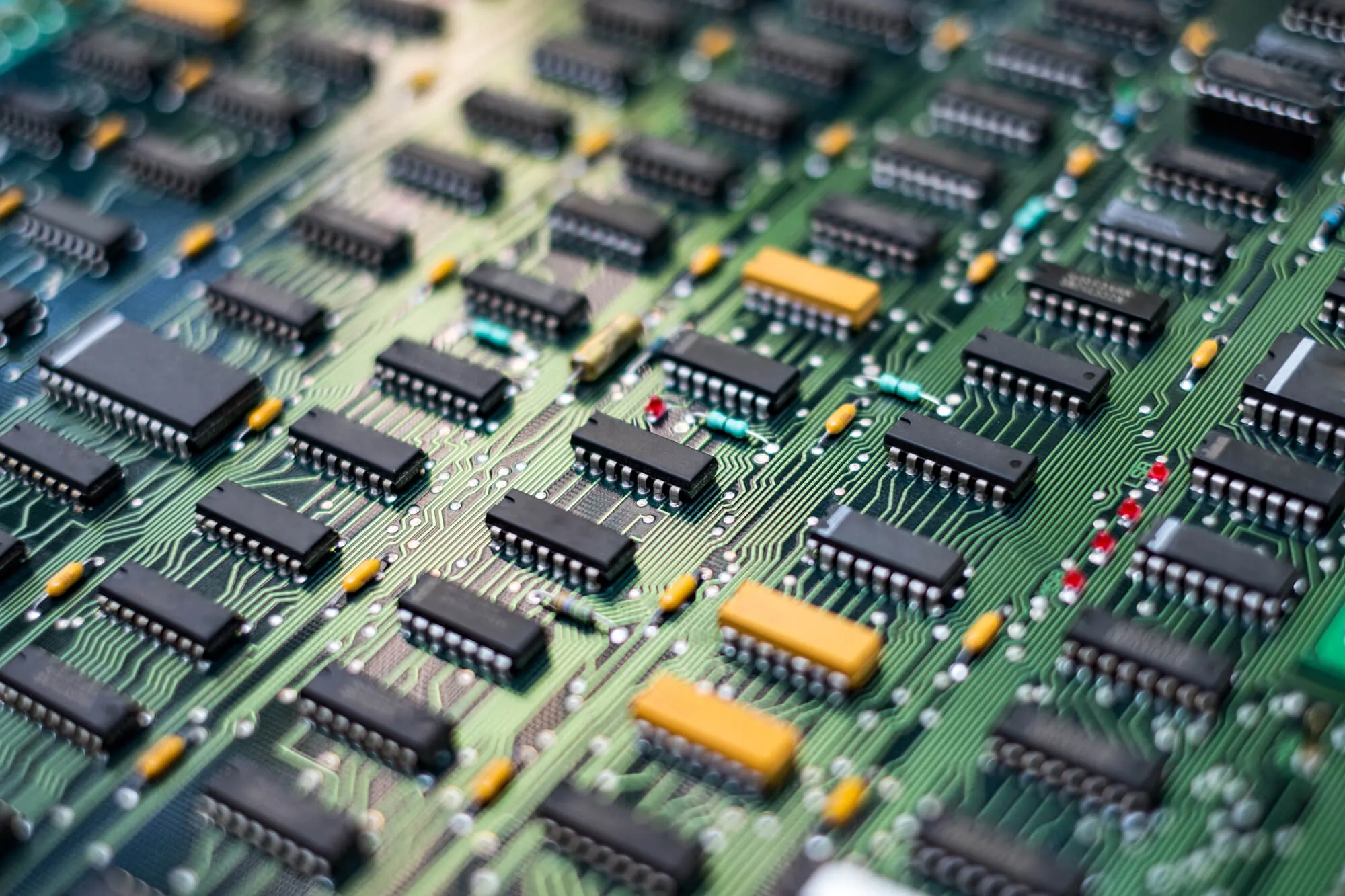
Thin wafers are used in various applications, including advanced microelectronics, MEMS (Micro-Electro-Mechanical Systems), power devices, photonics, and flexible electronics. They play a crucial role in enabling miniaturization, improved performance, and enhanced functionality of various electronic devices.
Ultra-thin silicon wafers are characterized by their reduced thickness, offering advantages such as improved flexibility, higher integration density, and enhanced performance. These wafers find applications in various semiconductor technologies, including microelectronics, sensors, and optoelectronics. Achieving precise thickness control and uniformity is critical for their successful manufacturing.
Manufacturing ultra-thin silicon wafers presents several significant challenges. One major obstacle is the delicate nature of the wafers, making handling and fragility issues paramount. Additionally, attaining precise thickness and uniformity during the thinning process is complex. Controlling wafer warpage, bowing, and reducing defects and impurities are key challenges to overcome.
The industry has witnessed remarkable innovations that tackle the challenges associated with ultra-thin silicon wafer manufacturing. Advanced wafer thinning techniques, including grinding, etching, and polishing, have been developed for precise thickness control. Thin film transfer technologies, such as bonding and layer transfer, offer alternative approaches to obtaining ultra-thin wafers.
Novel materials and substrates with improved mechanical stability have been explored, ensuring enhanced durability and reliability. Surface treatment methods have also been refined to enhance wafer quality and reliability.
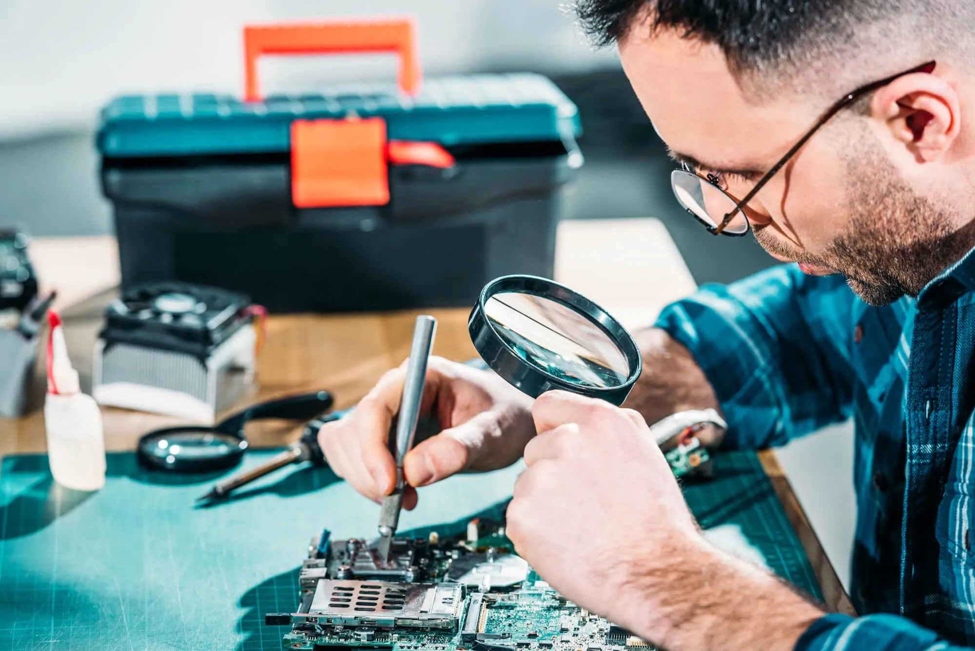
Accurate metrology and characterization play a vital role in ensuring the quality of ultra-thin silicon wafers. Various measurement techniques assess thickness and uniformity, while defect inspection and detection methods help identify potential issues. Evaluating mechanical properties and stress within ultra-thin silicon wafers aids in optimizing their performance.
Process optimization is crucial to consistently producing ultra-thin silicon wafers. Employing robust process control and monitoring strategies enhances uniformity and thickness control. Continuous improvement efforts, including defect reduction and quality enhancement measures, contribute to higher yield rates. Statistical process control and data analytics further assist in achieving operational excellence.
Significant advancements have been made in equipment and tooling to address the challenges associated with ultra-thin silicon wafer manufacturing. Specialized wafer handling and support systems have been developed to cater to the fragility of ultra-thin wafers. Cutting-edge thinning equipment with higher precision and automation capabilities aids in achieving the desired thickness and uniformity. Advanced surface treatment and cleaning technologies ensure optimum wafer quality.
Compliance with industry standards and specifications is essential to maintain consistency and quality in ultra-thin silicon wafer manufacturing. Adhering to thickness specifications, industry regulations, and environmental and safety considerations are paramount in ensuring responsible manufacturing practices.
The semiconductor industry thrives on collaboration and knowledge sharing. Manufacturers, researchers, and equipment suppliers actively collaborate to share best practices, lessons learned, and technological advancements. Industry consortiums and conferences play a vital role in fostering innovation and problem-solving.
The journey towards ultra-thin silicon wafer manufacturing continues to evolve. Ongoing research focuses on further improving thickness control, uniformity, and defect reduction. Advancements in thin film transfer technologies and exploration of alternative substrates hold promise for future advancements.
Additionally, developing new materials and processes for ultra-thin wafer manufacturing is an area of active exploration, aiming to enhance the performance and capabilities of next-generation semiconductor devices.
Through advancements in wafer thinning techniques, thin film transfer technologies, materials, and surface treatments, manufacturers have made significant progress in addressing these challenges. Precise thickness control, uniformity, and minimizing defects and fragility are critical to achieving high-quality ultra-thin wafers. Collaboration, knowledge sharing, and adherence to industry standards further drive advancements in this field.
The continuous pursuit of innovation and refinement in ultra-thin silicon wafer manufacturing sets the stage for developing next-generation semiconductor devices. As research and development efforts continue, we can anticipate further improvements in thickness control, enhanced mechanical stability, and the exploration of alternative substrates.
With these advancements, ultra-thin silicon wafers will play a pivotal role in shaping the future of semiconductor technology, enabling more advanced and sophisticated electronic devices across various industries.
At Wafer World, our team can provide silicon wafers to help you develop existing or new technologies. Give us a call today to learn more about our products.


