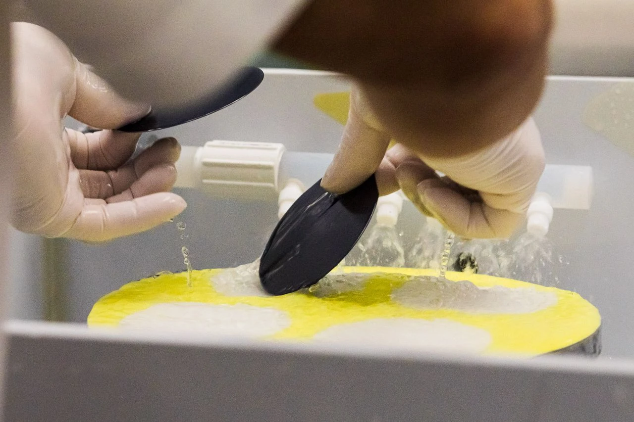
As semiconductor technologies continue evolving, manufacturers and researchers increasingly rely on materials with tighter tolerances and smoother surface finishes. A double side polish wafer provides enhanced flatness and surface quality that supports demanding applications across semiconductor fabrication, optics, and precision device manufacturing. These wafers are carefully processed to achieve polished surfaces on both sides, helping improve consistency during advanced production processes.
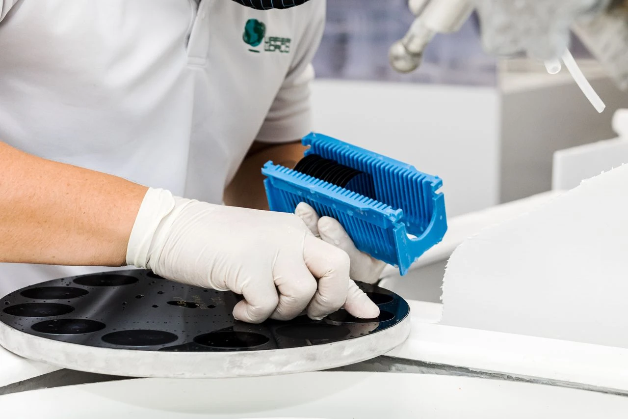
Double-side polishing is a manufacturing technique that simultaneously smooths and refines both wafer surfaces. This process helps improve thickness uniformity, surface flatness, and overall wafer stability.
Compared to single-sided polished wafers, double-sided polished wafers often offer better compatibility with applications that require precise alignment or dual-surface functionality. The polishing process also helps reduce surface irregularities that could interfere with sensitive semiconductor operations.
Polished wafers play a major role in semiconductor fabrication environments where precision directly impacts device performance. Smooth surfaces help support lithography, deposition, and etching processes used in advanced chip production.
Microelectromechanical systems (MEMS) often require wafers with highly controlled thickness and surface quality. Double-sided polished materials can help improve device accuracy and manufacturing consistency.
Optical technologies also benefit from polished wafer surfaces. Applications involving photonics, imaging systems, and optical sensors often depend on low surface defect levels and stable wafer geometry.
Engineers and procurement teams should evaluate several factors before selecting polished wafers for production or research use.
Surface roughness, flatness, and cleanliness directly affect wafer performance. Buyers should confirm inspection standards and polishing specifications with suppliers before ordering.
Different semiconductor applications may require specific substrate materials, orientations, or resistivity ranges. Understanding project requirements helps prevent compatibility issues during fabrication.
Polished surfaces require careful handling to avoid scratches or contamination. Proper packaging and cleanroom-compatible storage conditions help preserve wafer integrity during transportation and storage.
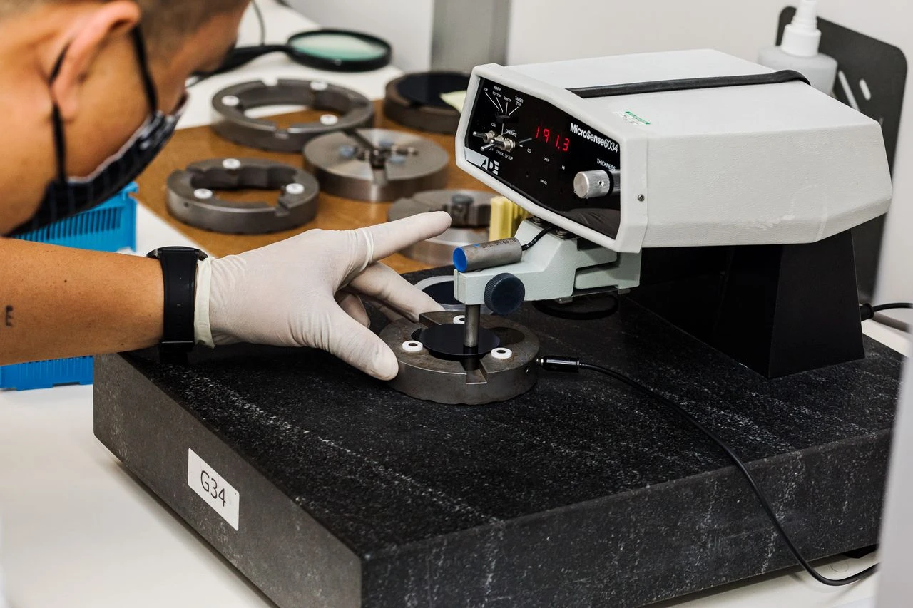
Selecting the right wafer materials can help improve fabrication reliability, process consistency, and long-term production efficiency. Whether supporting semiconductor development, MEMS fabrication, or optical technologies, polished wafer quality remains an important part of precision manufacturing success. At Wafer World, we continue to provide dependable wafer solutions designed to support advanced applications, with reliable material quality and industry-focused expertise. Contact us today!




