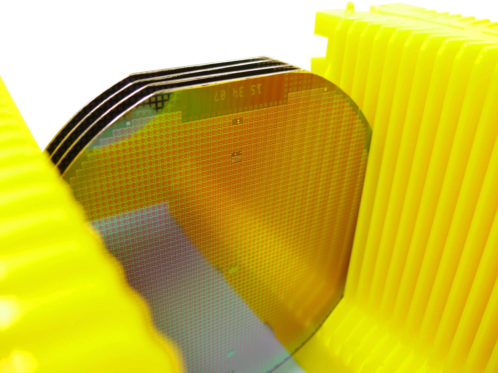
Silicon wafers are the building blocks of modern technology. They are the main component of integrated circuits and semiconductor devices. However, knowing the distinctions between standard and epitaxial silicon wafers is essential when choosing substrates from a silicon wafer supplier.
The decision between epitaxial and standard silicon wafers is influenced by several factors, including your particular application requirements, financial constraints, and the electrical properties needed.

Standard silicon wafers are uniform, single-crystal structures sliced from a silicon ingot. These wafers serve as the basic building blocks for many semiconductor applications. Silicon ingots are carefully grown using methods like the Czochralski process to ensure high purity. Some benefits of standard silicon include:
The growth of a crystalline layer on a crystalline substrate is known as epitaxy. In semiconductor manufacturing, epitaxy is the process of depositing a thin layer of single-crystal material onto a single-crystal substrate, with the deposited layer following the substrate's crystal orientation.
This epitaxial layer's thickness and doping concentration can be precisely controlled, improving electrical properties over conventional silicon wafers. There are two basic categories of epitaxial growth:
Moreover, epitaxial silicon offers several advantages, such as:
As you can see, the epitaxial and standard wafer manufacturing processes diverge. This makes them differentiate in various ways, such as:
The composition is the primary structural distinction between standard and epitaxial silicon wafers. Standard silicon wafers are made entirely from a single monocrystalline silicon ingot sliced into thin wafers. This gives them a uniform structure throughout, but may still contain imperfections such as dislocations or contamination from the crystal growth process.
In contrast, epitaxial silicon wafers consist of a thin, high-purity silicon layer—called the epitaxial layer—grown on top of a standard silicon substrate. This epitaxial layer has extremely low defect density and a uniform surface, allowing for precise control over doping concentrations.
Because of this, epitaxial wafers are better suited for advanced semiconductor devices where crystal quality and precise electrical characteristics are crucial.
Epitaxial wafers offer significant advantages over standard silicon wafers in terms of electrical performance. The controlled purity and structure of the epitaxial layer result in higher carrier mobility, reduced leakage currents, and improved breakdown voltages.
These qualities are essential for devices that operate under high voltage, high frequency, or extreme performance conditions—such as in RF circuits, power transistors, and advanced CMOS chips.
On the other hand, standard silicon wafers tend to suffer from greater defect density, impurity diffusion, and variations in doping levels. These imperfections can negatively affect the performance and reliability of high-end or high-speed electronic devices, making standard wafers less ideal for critical applications.
Doping is added to standard wafers during crystal growth for doping control, which produces more uniform but less precisely controlled doping concentrations. Conversely, doping on epitaxial wafers can be precisely regulated during the epitaxial growth, enabling abrupt junctions and complex doping profiles.
Regarding resistivity, standard wafers usually have values between <0.001 ohm-cm and >10,000 ohm-cm, uniform throughout the wafer. Different resistivity values can be found in the substrate and epitaxial layer of epitaxial wafers, with the epitaxial layer being customized to meet particular resistivity needs.
The two wafer types also differ in terms of quality and defect characteristics:
Standard wafers may have a variety of crystal defects, such as oxygen precipitates, dislocations, and slip lines, that result from the crystal growth process. Because epitaxial wafers are grown under carefully regulated conditions, they usually have fewer defects in the epitaxial layer than the substrate.
Standard wafers frequently need extra processing steps for impurity gettering, which removes impurities. In epitaxial wafers, the interface between the substrate and the epitaxial layer can be a natural gettering site, trapping impurities away from the active device area.
Standard wafers are simpler and less expensive, making them the go-to choice for large-volume manufacturing (such as solar cells and consumer electronics).
Epitaxial wafers require an additional, time-consuming CVD process and more precise control during manufacturing, leading to higher costs. Despite the cost, the added value in performance and reliability justifies their use in critical applications.
The choice between epitaxial and standard wafers depends largely on the intended application. Standard silicon wafers are widely used in cost-sensitive, high-volume products like solar panels, consumer electronics, and basic MEMS sensors.
Their lower cost and easier manufacturing process make them ideal for these devices, where performance requirements are moderate and reliability demands are not extreme.
On the other hand, epitaxial silicon wafers are typically used in applications that require high precision and performance. These include power electronics, high-voltage and high-frequency devices, analog and RF circuits, and cutting-edge CMOS technologies used in smartphones and advanced computing.
In these fields, the superior electrical properties and defect control offered by epitaxial wafers provide a clear advantage.

Both epitaxial silicon wafers and standard (bulk or Czochralski-grown) silicon wafers serve as building blocks for all of our technology. They are commonly used in the electronics and photovoltaic industries and serve similar purposes—but they differ significantly in terms of structure, fabrication process, cost, and performance characteristics.
The choice between epitaxial and standard silicon wafers depends heavily on the application requirements, budget, and performance expectations. If you need help figuring out which one works best for you, Wafer World can help. Contact us today and let’s explore all the available options!


