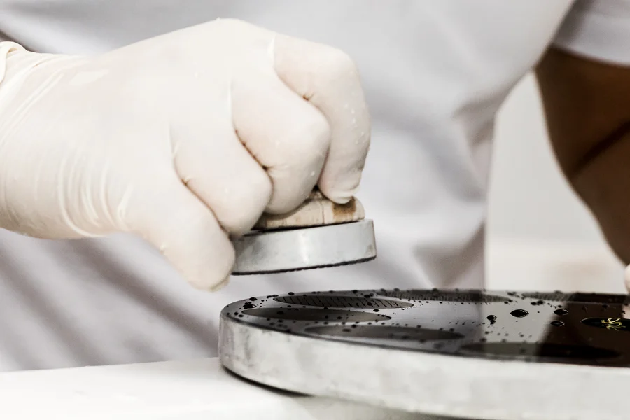
Producing a semiconductor wafer requires more than cutting a thin disc from a silicon crystal. In silicon wafer manufacturing, specialized equipment performs different tasks as the material moves through crystal growth, slicing, shaping, surface finishing, cleaning, and inspection. Each machine helps control the wafer’s physical condition before it is ready for its intended application.
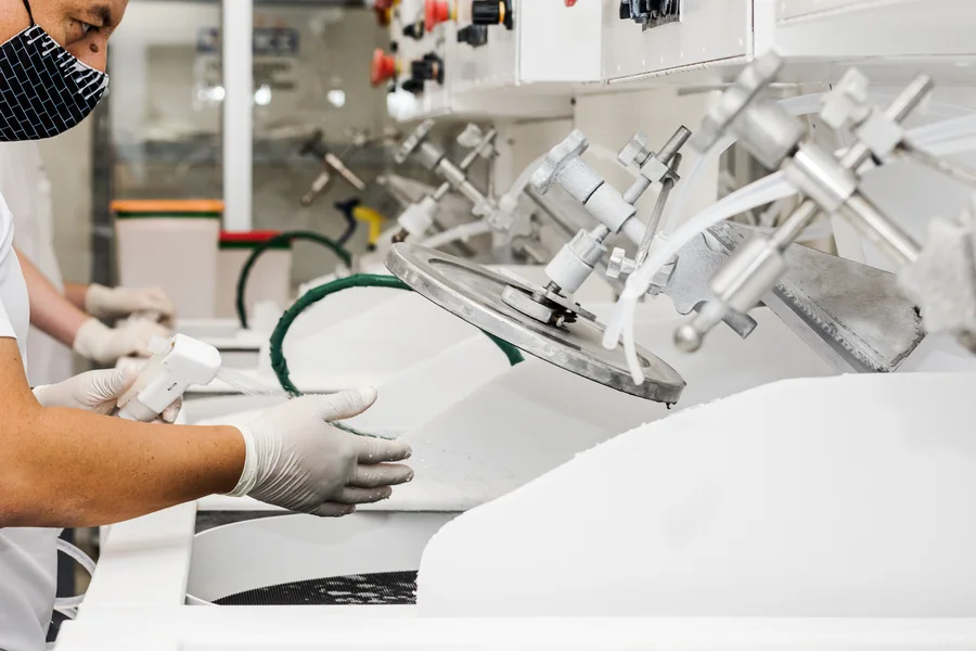
Before individual wafers can be made, silicon must first be formed into an ingot. The U.S. Department of Energy describes the Czochralski process as a method in which a crystalline seed contacts molten silicon and is slowly pulled upward to grow a monocrystalline ingot.
Crystal growth furnaces provide the controlled environment needed for this stage. Their role includes heating the silicon and supporting the controlled formation of crystals as the ingot develops. Equipment requirements can differ depending on the growth method and desired material characteristics.
Once an ingot is prepared, it must be divided into thin wafers. The Department of Energy notes that diamond-coated wire saws are used to slice silicon ingots into wafers. This operation creates the basic wafer shape, but the freshly sliced surfaces still require additional processing.
Equipment involved in turning an ingot into prepared wafers may include:
Slicing leaves’ surfaces and edges that are not yet in their finished condition. According to the Semiconductor Industry Association, wafer refinement can include edge grinding followed by double-side grinding or lapping. These operations help remove damage caused during slicing while bringing the wafer closer to the required thickness and flatness specifications.
Polishing equipment performs another important finishing function. NIST has documented specialized wafer-finishing systems used to achieve highly flat silicon surfaces. Such equipment integrates with measurement systems, enabling manufacturers to evaluate whether the resulting geometry meets established requirements.
This stage highlights why one machine cannot define wafer quality on its own. Slicing, grinding, lapping, and polishing perform distinct functions as the wafer progresses toward its required condition.
Processing can introduce particles and residues, making cleaning equipment another important part of wafer preparation. NIST lists dedicated single-wafer cleaning systems, wet benches, spin-rinse dryers, chemical mechanical polishing tools, and post-polishing wafer cleaners among the equipment used in nanofabrication facilities.
Metrology equipment then provides measurements needed to evaluate the finished substrate. NIST research on extremely flat wafers, for example, has used interferometry to measure total thickness variation. Rather than changing the wafer, these systems provide data that manufacturers can use to assess whether processing has produced the intended result.
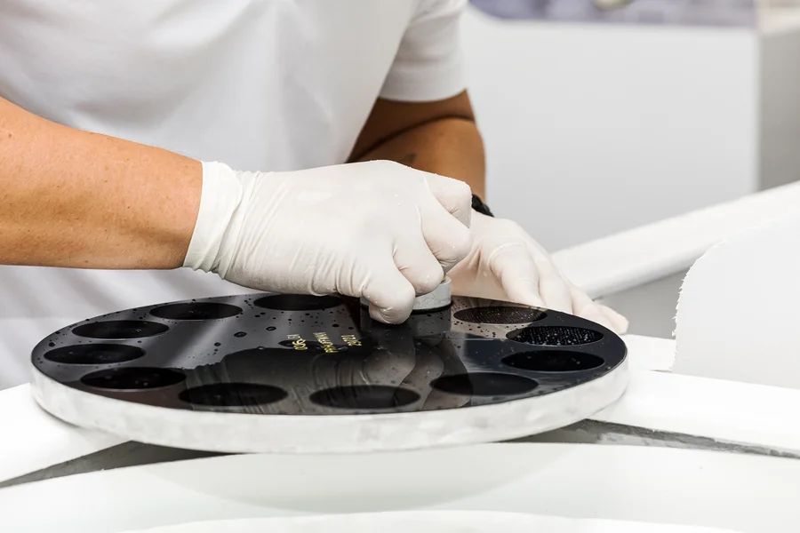
Understanding silicon wafer manufacturing equipment makes it easier to see how separate operations contribute to the finished substrate. Wafer World can help you review available wafer options and discuss the material, dimensions, surface condition, and other specifications relevant to your application. Contact us to schedule a consultation and discuss the wafer requirements for your next project.




