Silicon wafers are the foundation for many electronic gadgets in modern technology. Wafer world digs into the intriguing world of silicon wafer production, revealing the complex processes involved in changing raw materials into the crucial components that power our modern breakthroughs.
Raw Material Extraction and Purification: Silicon, the second most abundant element on the planet, is derived from silica, a compound found in sand. After extraction, the silica undergoes a purification process to remove impurities. A chemical reaction converts the purified silica into silicon, producing very pure polycrystalline silicon.
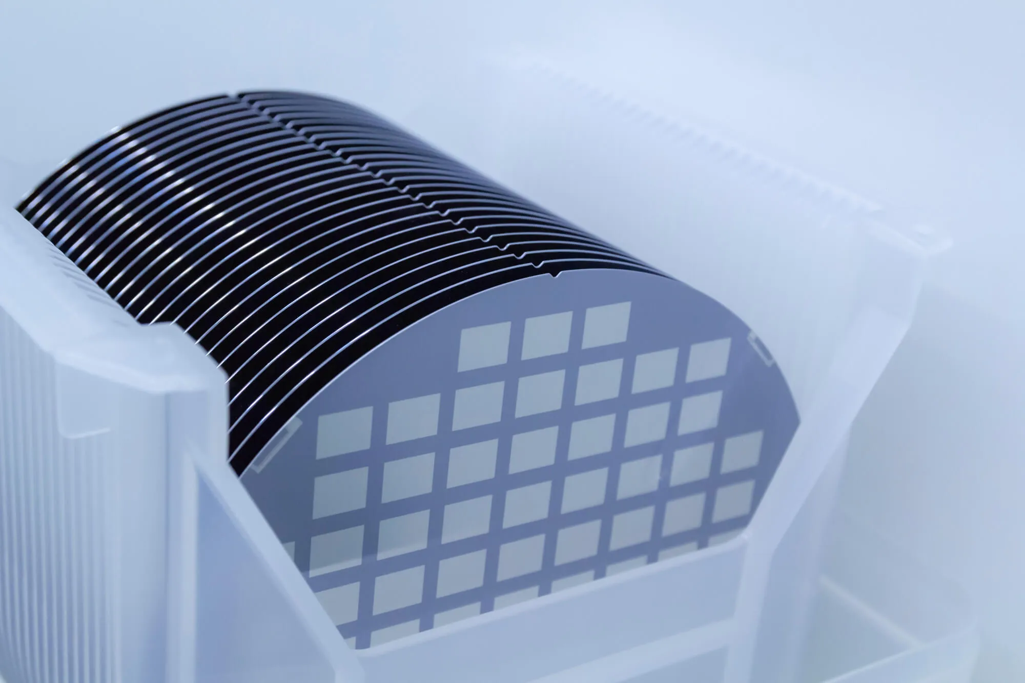
Crystal Growth: Polycrystalline silicon is melted and carefully cooled to form a large cylindrical ingot before being processed into single-crystal silicon wafers. This method, known as Czochralski growth, requires careful temperature control and modest cooling rates to prevent crystal flaws. The ingot is then split into thin wafers using a diamond-tipped saw.
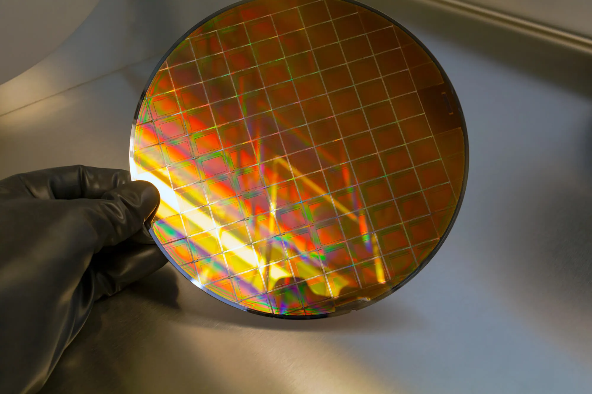
Wafer Surface Preparation: A variety of surface preparation procedures are performed on the sliced wafers. They are mechanically lapped and polished first to produce a smooth and level surface. Following that, chemical etching is used to erase any remaining surface flaws. A thin layer of silicon dioxide is formed on the wafer surface to provide electrical insulation and protection.
Photolithography and Doping:Photolithography, a key step in semiconductor manufacturing, involves precisely patterning circuits and structures on the wafer surface. A pattern is created by applying a light-sensitive substance called photoresist and exposing it to light via a mask. After that, the exposed portions are etched to remove or deposit materials, defining the required circuitry. Doping, or the insertion of impurities, is used to alter the electrical characteristics of certain wafer regions.
Looking to Understand More about Silicon Wafer Manufacturing?
Silicon wafer manufacturing is an intricate process that demands painstaking accuracy and strict quality control. This difficult journey delivers the foundation for our modern technological marvels, from raw material extraction to the detailed procedures of crystal growth, surface preparation, and circuit patterning.
Understanding the processes behind silicon wafer fabrication allows us to appreciate the ingenuity and expertise that support modern products, motivating future technological breakthroughs and developments in our increasingly interconnected world.
.webp)