
Ultra flat wafers are essential components across a variety of high-tech industries, from semiconductors to microelectronics. These wafers must meet extremely tight specifications to ensure they perform as expected. The manufacturing process for ultra flat wafers is complex and involves several steps to ensure precision, quality, and uniformity. Each stage is critical in achieving the ultra-flat surface needed for specialized applications, and quality control is closely monitored throughout production.
The production of ultra flat wafers begins with raw material selection, typically silicon or other semiconductors, which must be of high purity to ensure quality. The material is then sliced into thin wafers. The key to achieving ultra-flat wafers lies in the precise grinding, polishing, and etching processes that follow.
Grinding and polishing are done with incredible accuracy, often using diamond abrasive tools. This ensures that the wafers have a uniform thickness and smooth surface. After the initial shaping, ultra flat wafers undergo an additional process known as chemical-mechanical polishing (CMP) to refine flatness and remove microscopic defects that could affect performance.
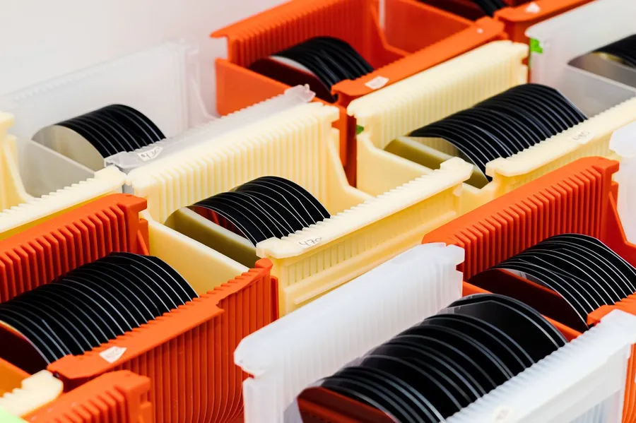
Throughout the production process, quality checks are performed at each stage to ensure that ultra flat wafers meet the required specifications. This includes inspecting the wafer’s thickness, flatness, and surface roughness. Specialized equipment measures and monitors these factors in real time, enabling manufacturers to make adjustments as needed to maintain precision.

If you’re looking for ultra flat wafers for your next project or need more information on their manufacturing process, contact Wafer World today. We specialize in providing high-quality wafers for a variety of industries, ensuring that each one meets the strictest precision and quality standards. Call us now to discuss your specific needs and schedule an order.


