Despite semiconductors becoming more common than ever before in everyday items, the cost hasn’t dropped. This has left many companies looking for cheaper alternatives. Unfortunately, sometimes the cheaper alternative lacks the quality needed. That’s where reclaim wafers come in. Let’s take a look at the INP reclaim wafers process as well as the cost benefit.
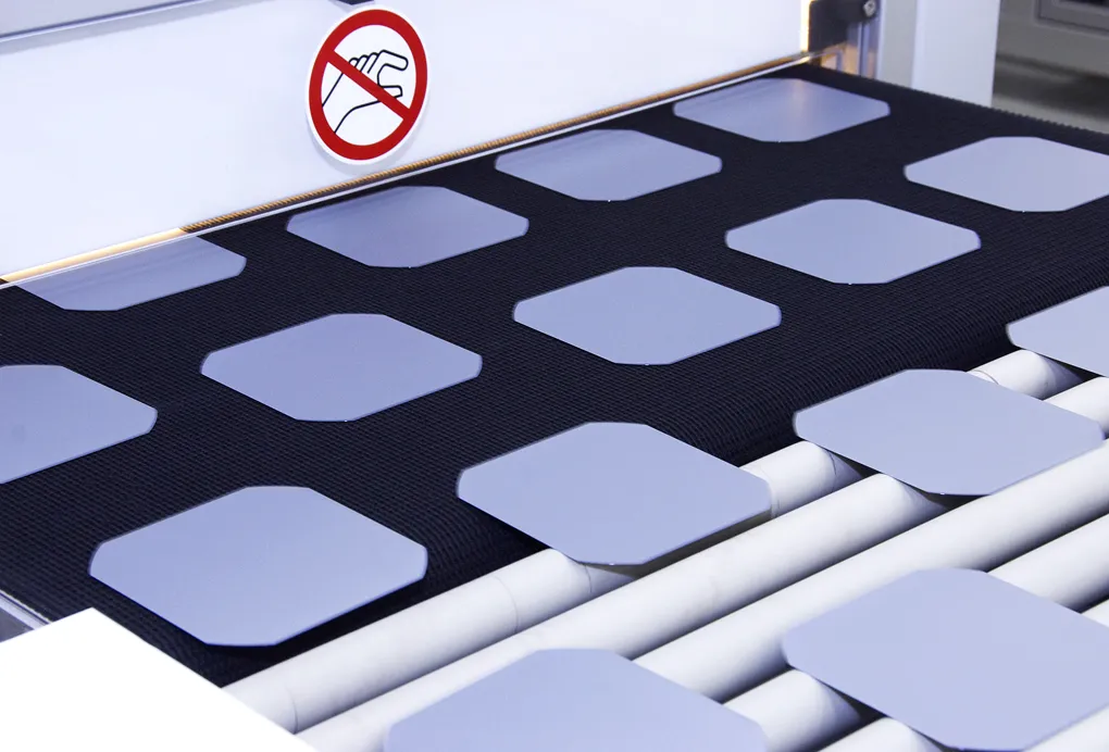
The wafer reclaim process begins with a visual inspection of incoming wafers for fatal flaws such as chipped edges or serious scratches. If a wafer passes this initial test, it is then measured for thickness to ensure that sufficient material exists. After the inspection, the wafer then goes through the chemical stripping process. This process removes the thin films from the wafer. After that it is polished, chemically cleaned, washed, rinsed with ultra-pure deionized water, and dried using both industry standard and proprietary techniques.
Reclaimed wafers can significantly cut expenses for both chip makers and semiconductor equipment manufacturers. A reclaim wafer is typically a third of the cost of a new wafer. The biggest cost savings are seen in the 100-mm through 300-mm wafer sizes. Depending on starting thickness, most wafers can be reclaimed several times. This can lead to even more of a cost savings.
At Wafer World, not only do we offer brand new semiconductor wafers to our clients but we also offer reclaimed ones as well. So, no matter what the project or budget, we have the wafer that you need. Contact us today to learn more and to place an order.


