Indium phosphide is a semiconducting material similar to GaAs and silicon but is very much a niche product. It’s very effective at developing very high-speed processing and is more expensive than GaAs because of the great lengths to gather and develop the ingredients. Let’s take a look at some more facts about indium phosphide as it pertains to an InP Wafer.
Indium Phosphide Facts
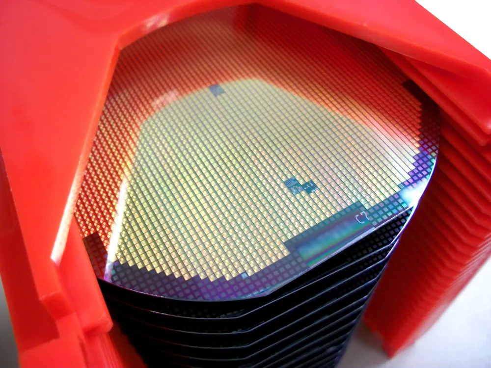
Indium phosphide (InP) includes phosphorus and indium and is a binary semiconductor.
It has a zincblende crystal structure similar to GaAs and almost all the III-V semiconductors.
It has superior electron velocity due to which it is used in high-frequency and high-power electronics.
Indium phosphide is also used as a substrate for optoelectronic devices.
Molecular weight: 145.792 g/mol
Melting point: 1062 °C (1943.6 °F)
It can be used for virtually any electronic device that requires high speed or high power.
It has one of the longest-lived optical phonons of any compound with the zincblende crystal structure.
InP is the most important material for the generation of laser signals and the detection and conversion of those signals back to electronic form.
Are You Looking for an InP Wafer?
At Wafer World, we are proud to offer indium phosphide wafers for all different kinds of projects. If you are looking for InP wafers, contact us today to learn more about how we can work with you to get you the indium phosphide wafers you need for your next project.