
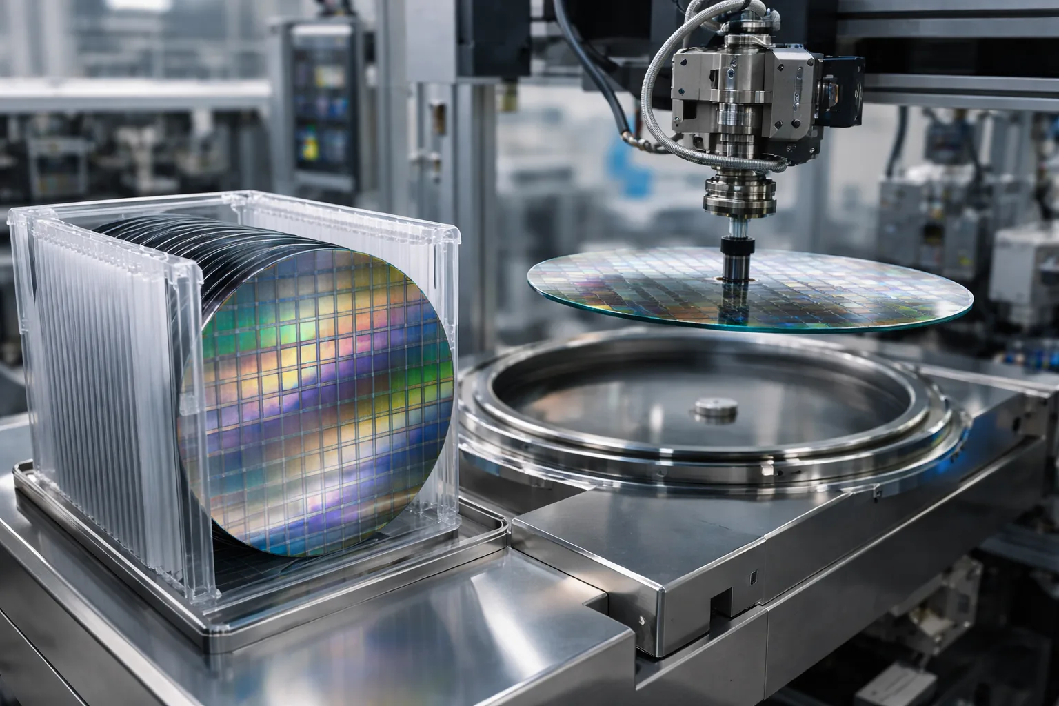
The InP wafer (Indium Phosphide wafer) is becoming an increasingly vital component in the semiconductor industry. Due to its unique properties, it is essential for a range of high-performance applications, including telecommunications, photonics, and high-frequency electronics.
Unlike traditional semiconductor materials, such as silicon, InP wafers excel in high-frequency and high-speed performance, making them indispensable for next-generation technologies.
With an ever-growing demand for faster, more efficient devices, the InP wafer market is seeing significant expansion.

The global market for InP wafers is on an upward trajectory, fueled by several key factors. As industries demand faster, more efficient devices, the need for high-quality semiconductors is growing.
The demand for InP wafers is being significantly driven by the rise of 5G technology. As 5G networks begin to roll out globally, there is a pressing need for high-performance semiconductors capable of operating at higher frequencies.
InP wafers are ideally suited for these applications due to their superior performance in high-frequency environments, making them an essential material for 5G infrastructure.
Another key growth factor for the InP wafer market is the rapid development of photonics and optoelectronics. In fields such as fiber optics and laser technology, InP wafers are widely used to fabricate devices for high-speed data transmission and light-based technologies.
Their exceptional properties, such as high electron mobility and optical characteristics, make them the material of choice for cutting-edge optical systems.
The global push for faster, more efficient computing devices, from smartphones to AI systems, is leading to an increased reliance on high-performance materials like InP wafers.
With industries such as automotive, AI, and IoT relying on faster data processing, the need for advanced semiconductor technologies is greater than ever. InP wafers are at the forefront of this demand due to their superior performance in high-frequency and high-speed applications.
While the InP wafer market shows immense growth potential, it faces several challenges that could hinder its widespread adoption and manufacturing.
Compared to other semiconductor materials, InP wafers are more expensive to produce. The manufacturing process is more complex, and the raw materials involved are costly.
This high production cost can deter companies from using InP wafers at higher volumes, particularly in applications where cost is a significant concern.
One of the key challenges for the InP wafer market is the limited availability of raw materials, particularly Indium. Indium is not as readily available as other semiconductor materials, such as silicon, which can create supply chain constraints.
Geopolitical factors and fluctuations in material costs can also impact the production of InP wafers.
While InP wafers offer superior performance, they still face certain technological limitations. For example, achieving uniform thickness and minimizing material defects during production remains challenging.
Additionally, manufacturers must continue to refine their processes to scale up production while maintaining quality.
The future for the InP wafer market looks promising, as technological advancements continue to shape the landscape.
As the world shifts toward advanced technologies such as AI, quantum computing, and autonomous vehicles, demand for high-performance materials, such as InP wafers, is expected to increase.
These emerging fields require semiconductor materials capable of handling complex tasks at high speeds, making InP wafers a critical component for innovation in these areas.
To address the high production costs of InP wafers, ongoing advancements in manufacturing processes are essential. New technologies that improve efficiency and reduce production costs are expected to make InP wafers more accessible for broader applications.
As economies of scale take effect, the price of InP wafers will likely decrease, enabling their adoption across more industries.
The use of InP wafers in consumer electronics is still in its early stages, but the potential for expansion is considerable.
As demand for faster, more efficient electronic devices grows, InP wafers will likely be integrated into more consumer products, from smartphones to wearables, enabling enhanced performance in everyday devices.
The InP wafer market is poised for substantial growth, driven by technological advancements and rising demand across industries such as telecommunications, photonics, and high-performance computing.
While challenges such as high production costs and limited material availability persist, innovations in manufacturing and technological advancements promise to address them. As the world continues to embrace faster, more efficient technologies, InP wafers will play a crucial role in shaping the future of electronics and communications.
As the InP wafer market grows and evolves, staying ahead of technological trends is essential for businesses involved in semiconductors, telecommunications, and electronics.
If you're looking for insights into how InP wafers can enhance your product development or are interested in exploring cutting-edge semiconductor solutions, reach out to Wafer World. Our team can help you navigate this fast-moving market and leverage the potential of InP wafers for your next project.


