Silicon isn’t the only type of wafer you can employ for your project or business. There are a few other types like an InP wafer and a GaAs wafer. These wafers are known for its superior properties in electrical and thermal fields compared to silicon and GaAs. That is why they’re in demand for high-power electronics. If your business or project has something to do with high-power or high-frequency electronics, then InP wafer is the type of wafer you’re looking for. Here are the things you need to know about InP wafers:
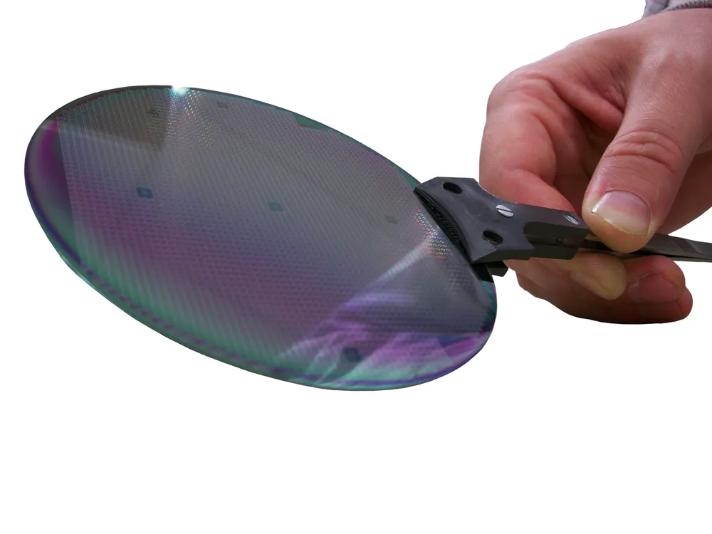
An InP wafer begins with an indium phosphide crystal which is grown through two methods: the LEC or Liquid Encapsulated Czochralski method or VGF method.
These wafers are known for their superior electron velocity, thermal, and electrical properties. They have high electron mobility, high frequency, reduced power consumption, reduced noise performance, and high thermal conductivity compared to GaAs wafers and Silicon wafers.
They can be used in optoelectronic devices. It functions as a substrate for epitaxial indium gallium arsenide. It also has one of the most longest-lived optical quanta of lattice vibrations present in crystals of any compound.

Get quality InP wafer from a wafer company you can trust. At Wafer World, we are dedicated to providing all types of high-quality wafers for all our clients worldwide. Call us today for any wafer specification requests or visit our website to purchase wafers online. We look forward to hearing from you.


