Laser marking is essential for the reclaim and reuse of indium phosphide (InP) wafers, as traceability, process control, and material integrity are all critical requirements for this process. Unlike silicon, InP is a fragile, high-value compound semiconductor with stringent requirements for surface and thermal stability. Choosing the incorrect marking method can permanently damage the InP reclaim wafer, rendering it unsuitable for high-performance photonic and RF applications.
To prevent that, understanding how laser marking works for InP reclaim wafers, what makes InP different, which laser technologies are recommended, and how to avoid costly defects while maintaining full traceability is crucial for manufacturers.
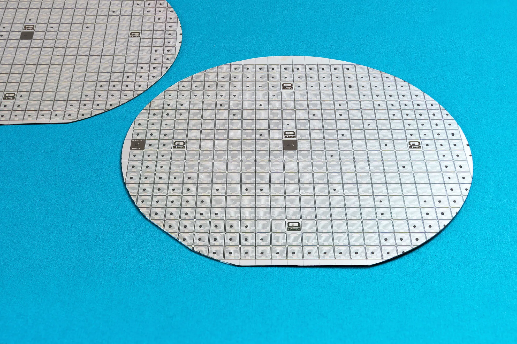
InP wafers, or indium phosphide wafers, are semiconductor materials made from indium and phosphorus compounds. Their single-crystal structure characterizes them and is primarily used in high-speed electronic devices and optoelectronic components, such as lasers, photodiodes, and solar cells, where performance depends heavily on crystal quality and surface condition.
They are also widely used in telecommunications and microwave technology, particularly fiber-optic communication systems. InP wafers have a stable structure and they crystallize in a face-centered cubic structure, like other III-V semiconductors.
Nevertheless, just as they come with benefits, InP wafers present some handling challenges. During the reclaim process, wafers are stripped, polished, inspected, and reintroduced into production—often multiple times. However, this can be challenging, because InP has:
As a result, traditional marking methods for silicon wafers cannot be used blindly on InP reclaim wafers.
Laser marking offers non-contact, contamination-free identification that remains intact even after cleaning, polishing, and high-temperature processing steps. It has become a fundamental step in wafer manufacturing—often demanded by clients, quality standards, and even laws in critical industries, as well.
So, when marking complex compounds like indium phosphide, it can be easy to think, can’t I just skip this step? However, for reclaim operations, marking is not optional—it is essential for:
For InP reclaim wafers, laser marking must strike a precise balance between readability and material safety.
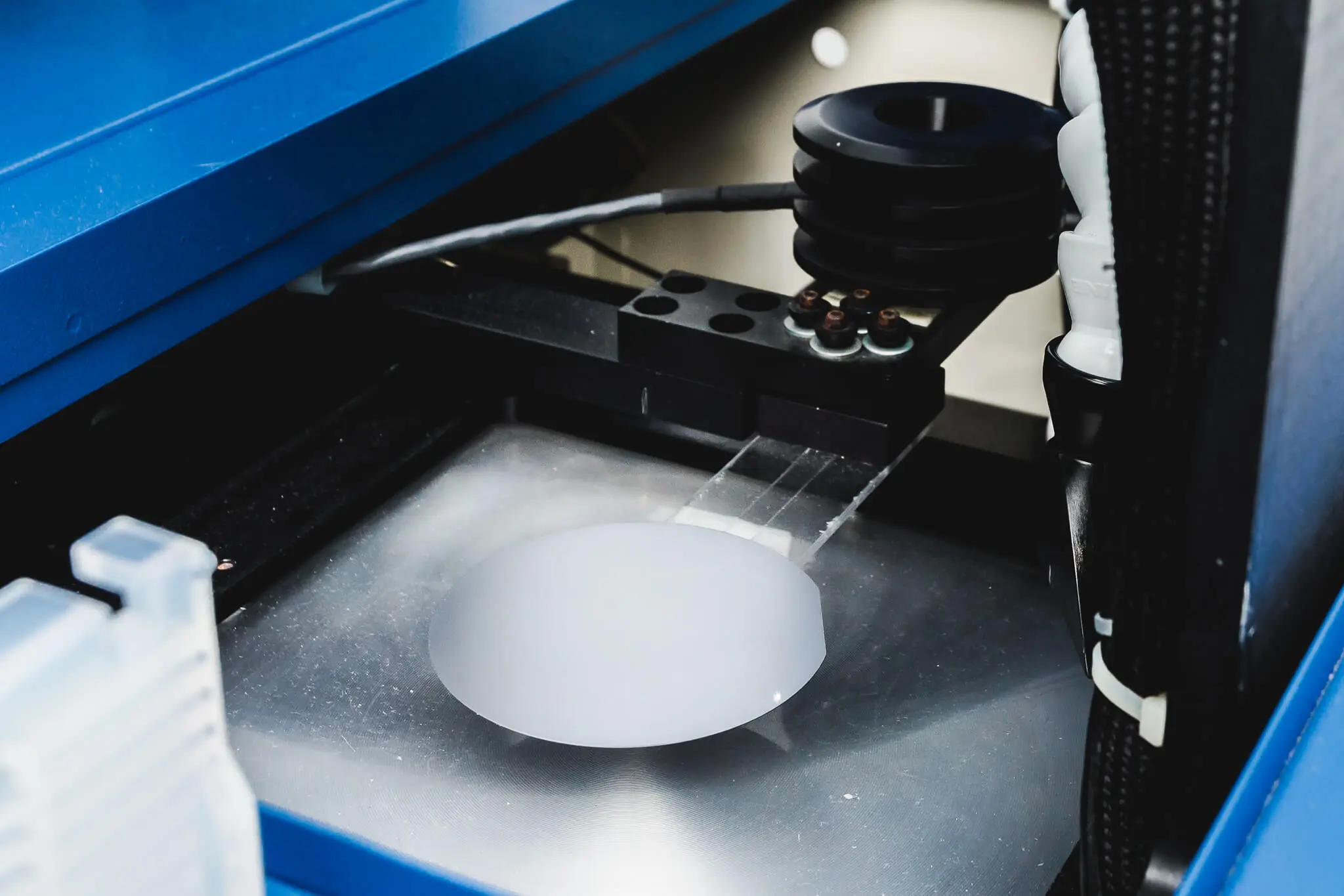
Unlike mechanical marking techniques, laser marking uses a focused laser beam to modify the wafer surface locally. This helps minimize any impact on the wafer’s structure, ensuring trackability while maintaining the material’s integrity.
Still, wafer marking can have its risks. Depending on the wavelength, pulse duration, and power density, the laser can:
For InP wafers, the goal is to achieve surface-level modification only, thereby avoiding subsurface damage or microcracks that can propagate during downstream processing. So, what methods are recommended to achieve this?
Ultrashort-pulse lasers are strongly recommended for InP reclaim wafers because they minimize thermal diffusion, reducing heat-affected zones and preventing micro-fractures and crystal damage. These lasers rely on “cold ablation,” where material modification occurs faster than heat can spread into the lattice.
They’re the best choice for:
InP absorbs laser energy differently from silicon. Improper wavelength selection can cause issues such as excessive heating, surface melting, and phosphorus outgassing. For that reason, selecting only infrared or green wavelengths is recommended.
Additionally, experts recommend you:
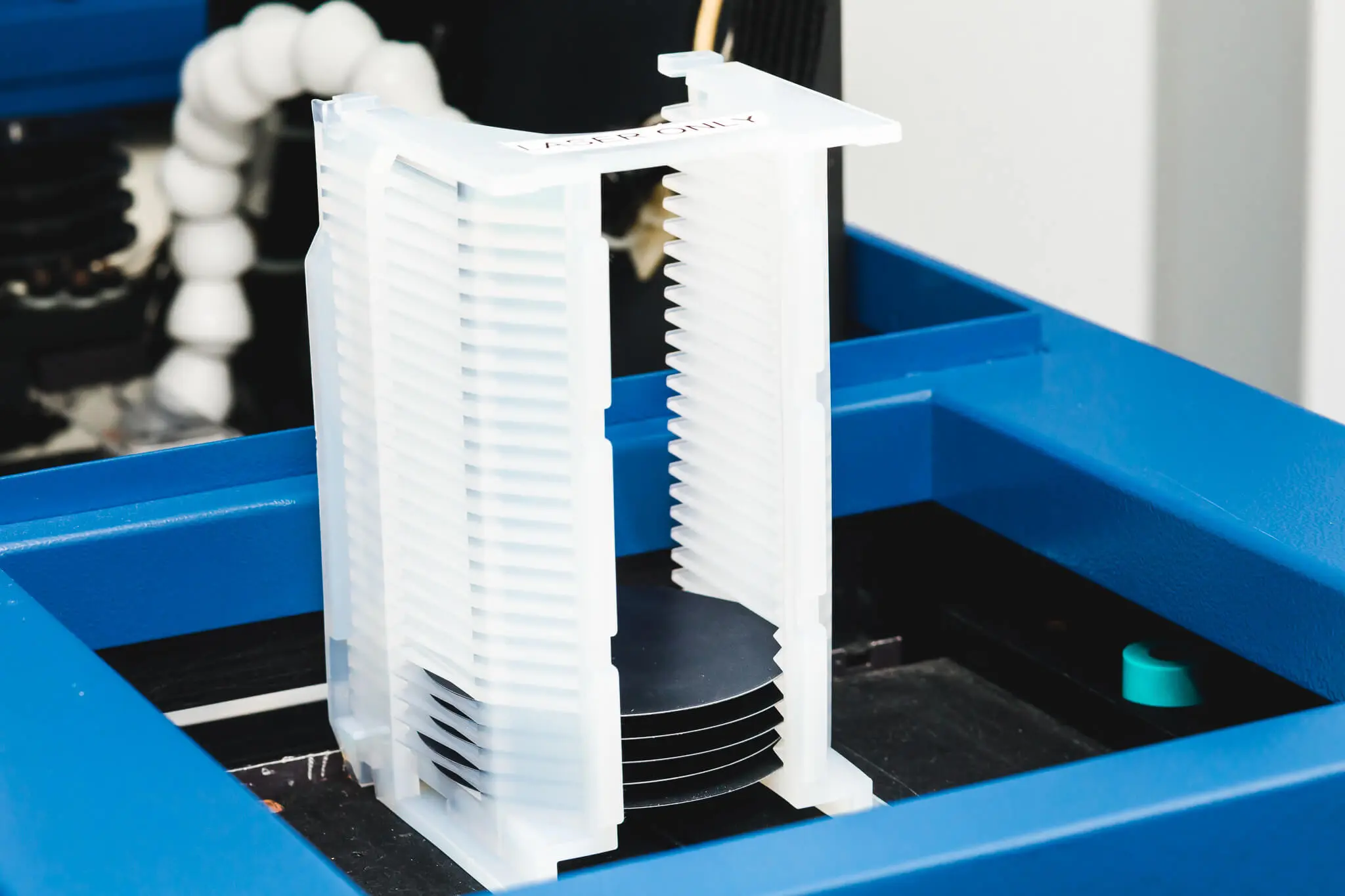
For InP reclaim wafers, edge marking is the industry standard. This method helps ensure zero impact on active device areas and lower stress concentration. Additionally, it facilitates removal during repolishing, if needed.
Frontside marking is generally discouraged unless absolutely required—and only with ultrashort pulses.
In reclaim workflows, markings must survive:
Therefore, it can be easy to believe that the most effective marking methods are ideal. That is not necessarily true. Excessive marking depth increases crack initiation risk, so it’s better to use shallow, high-contrast marks, optimized repetition rate, and automated vision inspection post-marking.
When done right, laser marking can offer several benefits for InP reclaim wafer manufacturers. Some of these include:
Laser marking systems can achieve micron-level accuracy, ensuring consistent placement even on smaller-diameter compound wafers.
No inks, no chemicals, no mechanical stress—critical for contamination-sensitive InP processes.
Properly executed laser marks remain legible without compromising reclaim yield or device performance.
Laser marking integrates seamlessly into reclaim lines, enabling:
No solvents or consumables, aligning with sustainability goals in semiconductor manufacturing.
Many reclaim losses occur due to silicon-centric assumptions. Avoid:
A single microcrack can render an InP wafer unusable for high-frequency or optical applications.
Not all laser marking systems are suitable for InP reclaim wafers. When evaluating suppliers, look for:
A supplier that understands InP physics—not just laser hardware—can prevent costly trial-and-error.
Laser marking for InP reclaim wafers is not a commodity process. It requires material-specific expertise, precise parameter control, and the right laser technology. When done correctly, laser marking enhances traceability without compromising wafer integrity—helping manufacturers reclaim, reuse, and maximize the value of one of the most expensive semiconductor substrates on the market.
If you are processing InP wafers, Wafer World can help. Contact us today to learn more about how we reclaim and laser mark our InP wafers.


