In the dynamic realm of semiconductor materials, where each element vies for a pivotal role in advancing technology, Indium Phosphide (InP) has emerged as a distinctive contender. Its unique properties make it a sought-after material in wafer production, driving innovations in electronics, optoelectronics, and telecommunications.
In this blog post, we will explore the fascinating landscape of the InP wafer, delving into the advantages that have propelled its popularity and the challenges that researchers and engineers must overcome.
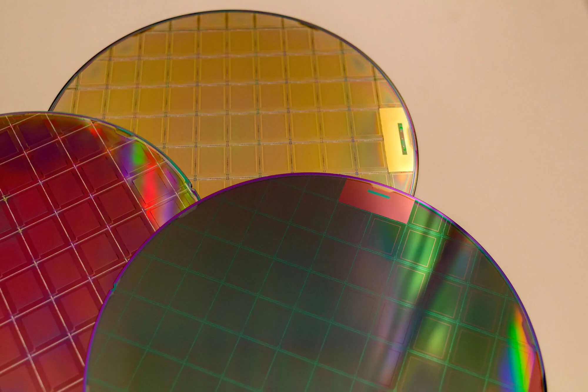
The semiconductor industry has experienced remarkable innovation and advancement over the past several decades. Integrated circuits and microchips have become progressively smaller, faster, and more powerful, enabling the creation of smaller, more capable, and affordable electronics. However, the pace of innovation brings both opportunities and obstacles.
InP's standout feature is its high electron mobility, a crucial factor in semiconductor materials. Electron mobility refers to the speed at which electrons move through a material in response to an electric field. InP's exceptional electron mobility contributes to the efficient functioning of electronic devices, making it particularly valuable in high-frequency applications.
InP's optical properties make it a star in the field of photonics and optoelectronics. Its direct bandgap allows for efficient light emission, making InP a preferred material for lasers, photodetectors, and modulators. The wavelength range covered by InP devices aligns with the needs of modern communication systems, further enhancing its relevance in the telecommunications industry.
InP's versatility extends across various applications, from high-speed transistors to light-emitting devices. Its adaptability allows it to play a role in both electronic and optical components, making it an attractive choice for integrated systems where diverse functionalities are crucial.
InP wafers exhibit remarkable stability across a range of temperatures. This property is especially valuable in applications where the semiconductor material must endure fluctuating environmental conditions without compromising performance. The ability of InP to maintain its integrity under varying temperatures enhances its reliability in real-world scenarios.
The high breakdown voltage of InP is advantageous in power electronics. Devices built on InP wafers can handle higher voltages without experiencing breakdown or failure. This characteristic is instrumental in designing robust and resilient power systems.
InP's excellent performance at small scales makes it ideal for the ongoing trend of miniaturization in electronics. As technology marches towards smaller and more integrated devices, InP wafers offer a promising solution for achieving enhanced functionality within compact form factors.
.webp)
While InP boasts impressive qualities, its production involves the use of indium, a relatively scarce and expensive material. The cost of indium can pose challenges for widespread adoption, especially in applications that require large-scale production. Researchers are actively exploring ways to mitigate these cost constraints through recycling initiatives and alternative fabrication methods.
Integrating InP technology with existing semiconductor technologies can be complex. Compatibility issues may arise when attempting to incorporate InP devices into established electronic systems. Overcoming these integration challenges requires a deep understanding of both InP's characteristics and the existing semiconductor landscape.
The production of InP wafers demands a high level of precision. The crystal growth process and wafer slicing must be executed meticulously to ensure the desired material properties. Achieving the necessary precision in manufacturing can be resource-intensive, impacting both time and cost factors.
As with any semiconductor material, achieving high device yield and reliability is a critical concern. InP devices must undergo stringent testing and quality control measures to ensure consistent performance. Researchers continually explore methods to enhance the yield and reliability of InP-based devices, addressing issues such as defect density and manufacturing variations.
The production and disposal of semiconductor materials, including InP, raise environmental considerations. Indium extraction and purification processes can generate environmental pollutants. Researchers and industry players are actively working toward sustainable practices, seeking to minimize the environmental impact of InP wafer production.
As demand for InP wafers rises, the challenge of scaling up production becomes more pronounced. Innovators are exploring ways to increase the yield and efficiency of InP fabrication processes, ensuring a stable supply chain to meet the growing needs of industries relying on this semiconductor material.
One of the frontiers in semiconductor technology involves integrating multiple functionalities onto a single chip. InP's versatility positions it as a key player in this quest for multifunctional devices. However, challenges persist in seamlessly integrating disparate functions onto a single InP-based platform. Researchers are actively addressing these challenges to unlock the full potential of InP in integrated systems.
As the advantages and challenges of InP wafers become increasingly apparent, researchers and engineers are navigating the landscape with optimism and determination. Collaborative efforts across academia and industry aim to unlock the full potential of InP, pushing the boundaries of what is possible in the semiconductor world.
In addressing the challenges, advancements in manufacturing techniques, recycling initiatives, and improved integration strategies are on the horizon. Researchers are exploring innovative solutions to enhance the cost-effectiveness of InP production, ensuring its benefits can be harnessed without imposing prohibitive economic constraints.
The integration of InP wafers into existing technologies requires a multidisciplinary approach, fostering collaboration between experts in materials science, electronics, and photonics. By overcoming compatibility challenges and streamlining integration processes, InP can seamlessly find its place in the ever-evolving landscape of semiconductor technologies.
Moreover, the environmental impact of InP production is a focal point for sustainability efforts within the semiconductor industry. Researchers are actively exploring eco-friendly alternatives and implementing responsible practices to mitigate the ecological footprint associated with InP wafers.

The advantages of InP wafers underscore their significance in shaping the future of semiconductor technologies. The challenges, while noteworthy, serve as opportunities for innovation and improvement.
As researchers and engineers continue to unravel the mysteries of InP, the semiconductor landscape stands poised for transformative breakthroughs, ushering in a new era of electronic and optoelectronic possibilities. Call us today!


