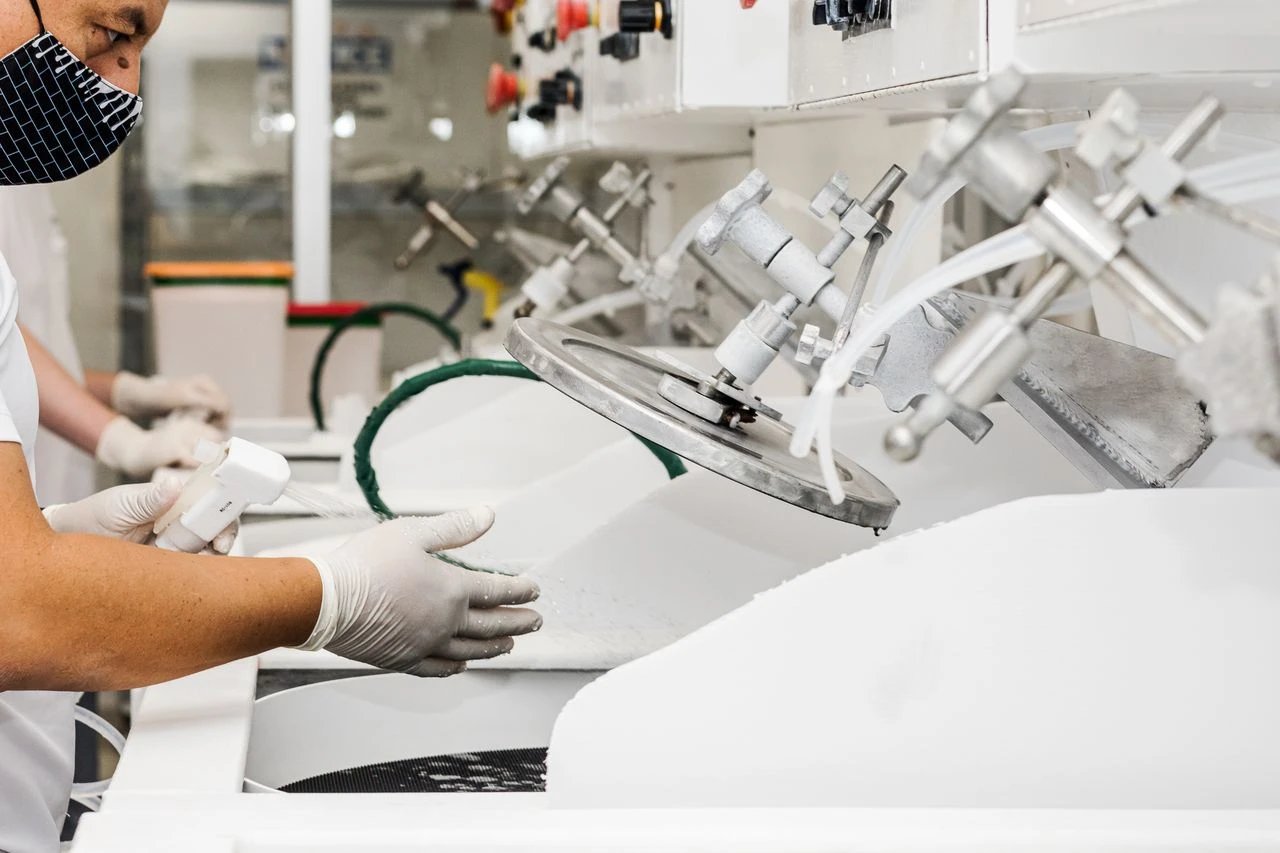
Modern electronics depend on carefully engineered materials that can support reliable electrical performance, thermal stability, and long-term durability. From semiconductors and solar cells to sensors and research equipment, silicon remains one of the most widely used materials in advanced technology. The silicon manufacturing process involves multiple highly controlled stages that transform raw quartz into polished wafers suitable for technical applications.
Producing wafers requires more than simply refining raw material. Manufacturers must maintain strict standards for purity, crystal structure, dimensional accuracy, and surface quality throughout every stage of production. Even small inconsistencies may affect fabrication efficiency, electrical conductivity, or overall product reliability.
As demand for semiconductors continues to grow across industries, understanding how wafers are produced can help organizations make informed sourcing and application decisions. Each stage of the process contributes to the performance of the finished material, from raw material preparation to final inspection.
Silicon production begins with quartz, a naturally occurring material composed primarily of silicon dioxide. Quartz is commonly mined from deposits that contain high levels of purity suitable for industrial processing.
The raw quartz is combined with carbon materials, such as coal or coke, and heated inside electric arc furnaces at extremely high temperatures. This process separates oxygen from the quartz and produces metallurgical-grade silicon.
Although metallurgical-grade silicon contains a high concentration of silicon, it still includes impurities that make it unsuitable for semiconductor applications. Additional purification stages are necessary before the material can be used in electronics or wafer fabrication.
To improve purity, manufacturers convert the material into chemical compounds, such as trichlorosilane. These compounds undergo controlled purification procedures that remove contaminants and unwanted trace elements.
After purification, the material is converted back into highly refined polysilicon. Semiconductor-grade polysilicon contains extremely low impurity concentrations, allowing it to support advanced electrical applications.
Purity standards are critical because even microscopic contaminants may affect conductivity, crystal formation, or device performance. Maintaining stable purification conditions helps ensure reliable downstream processing.
Once purified polysilicon is prepared, manufacturers begin crystal growth. This phase creates the large single-crystal structures used to produce wafers.
One of the most common methods is the Czochralski process. During this procedure, purified silicon is melted inside a crucible while a small seed crystal is slowly pulled upward and rotated. As the crystal rises, molten silicon solidifies around the seed, forming a cylindrical ingot.
The resulting crystal structure must remain highly uniform throughout the growth cycle. Temperature fluctuations, contamination, or growth instability can introduce defects that affect wafer quality.
Some applications require even higher purity levels and lower oxygen content. Float-zone processing addresses these needs by melting a localized region of silicon without using a crucible.
Because the material avoids direct contact with crucible surfaces, float-zone crystals often achieve superior purity and electrical performance. These wafers are frequently selected for power electronics, detectors, and specialized research environments.
Crystal orientation is also established during this phase. Common orientations include <100>, <110>, and <111>, each offering different properties for fabrication and device processing.
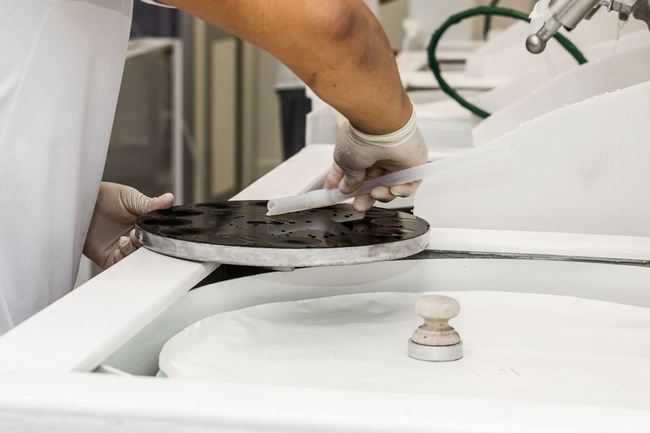
After crystal growth is complete, the ingot is carefully shaped and prepared for slicing. Manufacturers grind the ingot to achieve the desired diameter before cutting reference flats or notches that identify crystal orientation.
Diamond wire saws are commonly used to slice the ingot into thin wafers. Precision is essential because thickness variations may create challenges during later processing stages.
The sliced wafers initially have rough surfaces and mechanical stress from cutting operations. Additional processing steps are required to improve flatness, reduce damage, and prepare the material for polishing.
Wafer edges are shaped to reduce the risk of chipping or cracking during handling. Edge profiling also improves durability throughout transportation and fabrication.
Surface conditioning procedures remove saw marks and subsurface damage introduced during slicing. Grinding and lapping techniques help create smoother, more uniform surfaces before final polishing begins.
Thickness consistency is carefully monitored because dimensional stability directly affects lithography, coating, and automated handling performance.
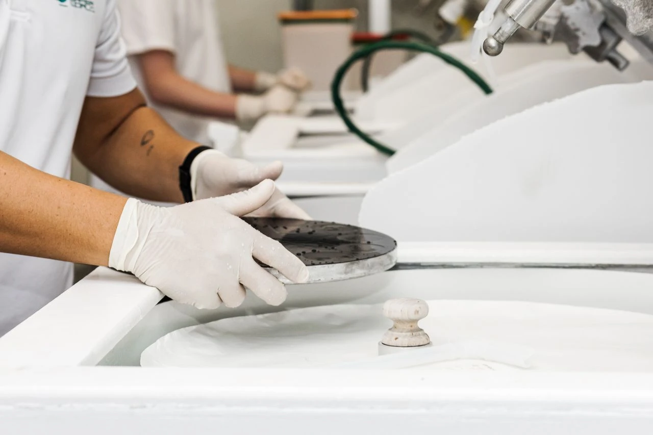
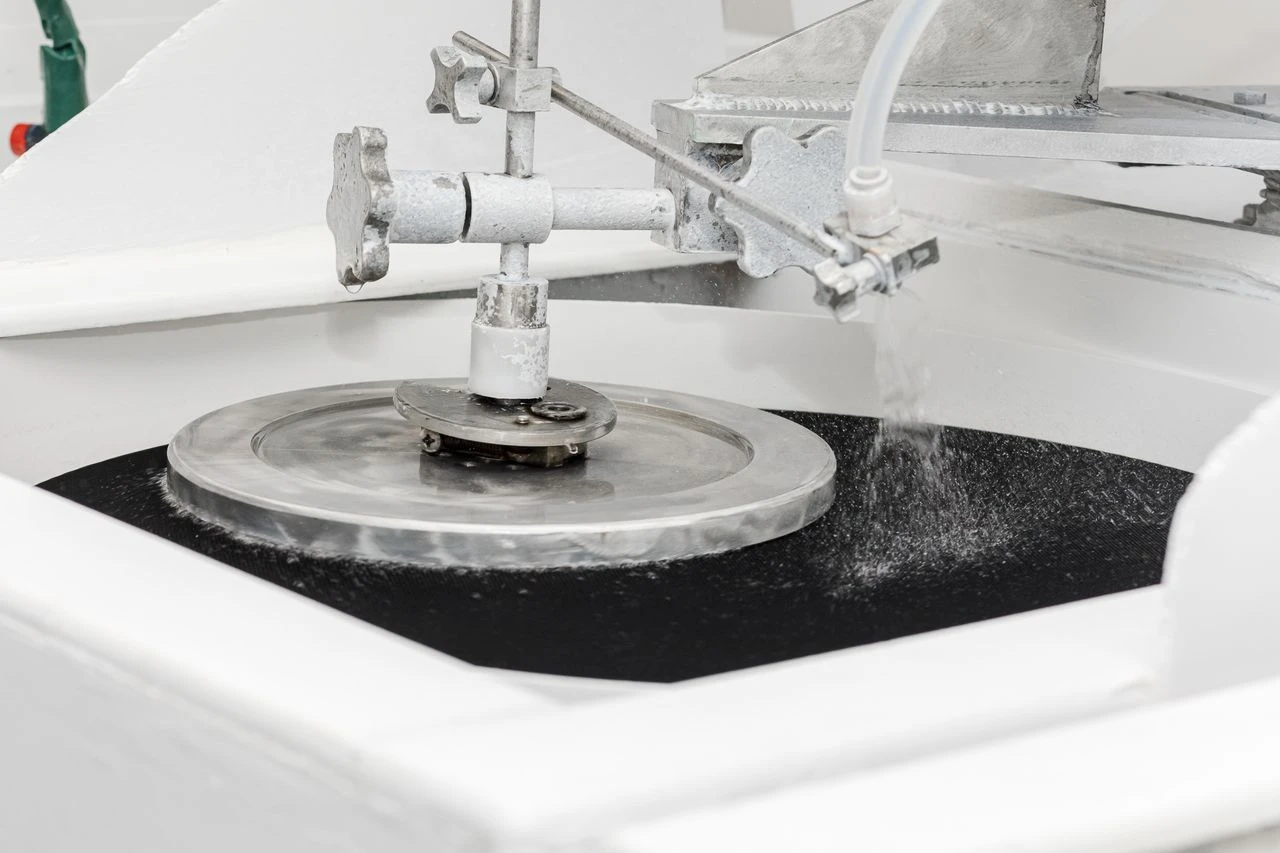
Polishing transforms rough wafers into highly smooth substrates suitable for advanced applications. Chemical mechanical polishing is often used to achieve mirror-like surfaces with minimal imperfections.
Single-sided polished wafers are commonly selected for applications where only one active surface is necessary. Double-sided polished wafers provide improved uniformity for more specialized fabrication processes.
Flatness measurements are especially important in semiconductor environments. Warp, bow, and total thickness variation must remain within precise tolerances to support reliable processing.
After polishing, wafers undergo extensive cleaning to remove particles, chemical residue, and organic contaminants. Cleanroom environments help minimize exposure to airborne particles during handling and packaging.
Contamination control remains essential throughout transportation and storage. Even tiny particles may interfere with deposition, etching, or photolithography procedures.
Manufacturers often use specialized packaging systems to protect wafers from moisture, static discharge, and physical damage before delivery.
Before wafers are approved for shipment, they undergo multiple inspection and testing procedures. Optical systems evaluate surface quality by identifying scratches, pits, haze, and other visible defects.
Electrical testing verifies resistivity levels, conductivity type, and crystal properties. These measurements help confirm that the wafers meet intended application requirements.
Automated metrology equipment is frequently used to measure thickness uniformity, flatness, and dimensional tolerances. Maintaining strict quality standards helps improve fabrication consistency and device reliability.
Traceability allows manufacturers and end users to track wafer specifications throughout production cycles. Documentation may include crystal orientation, resistivity ranges, polishing methods, and inspection data.
Stable process control also helps reduce batch-to-batch variability. Consistent production methods support reliable outcomes for semiconductor manufacturing, MEMS fabrication, and university research projects.
As technology applications continue to evolve, wafer producers must balance precision, efficiency, and scalability while maintaining strict quality standards.
The journey from raw quartz to finished wafers involves a series of highly controlled procedures designed to achieve precision, purity, and consistency. Organizations working with semiconductor devices, photovoltaic systems, or research applications benefit from understanding how wafer materials are refined, shaped, polished, and tested before reaching the final production stage.
If your team is exploring materials for silicon manufacturing, reviewing wafer specifications and production standards can help ensure more reliable long-term results. Wafer World provides silicon wafer solutions for technical, industrial, and research applications. Contact us today to discuss your project requirements or connect with our team for additional information.




