Semiconductors, or integrated circuits, are complicated mechanisms found in almost all types of electronic devices. The process that goes into the manufacturing of semiconductors can be difficult and time-consuming. It can also be important to know. Let’s take a look at wafer manufacturing and, specifically how semiconductors are made.
The first step in the manufacturing process is the actual production of the wafer. In this process, purified polycrystalline silicon is heated to a molten liquid. A small piece of solid silicon is placed on the molten liquid. As the silicon is slowly pulled from the melt, the liquid cools to form a single crystal ingot. The wafer is then processed through a series of machines, where it is ground smooth and chemically polished to a mirror-like luster.

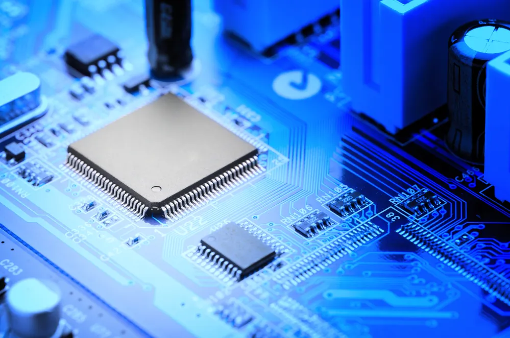
The most important step in the manufacturing process is the fabrication of the wafer. This is where the integrated circuit is formed in and on the wafer. The fabrication process, which takes place in a clean room, involves a series of steps and the process can take anywhere from 10 to 30 days to complete. The following steps are found in the fabrication process.
Wafer World is the best Silicon wafer manufacturer in the world. Let's learn more about Silicon Wafer manufacturing and Silicon Wafer processing step by step:
Surface grinding produces low-cost and high-quality wafers than its counterparts. It can partially or entirely replace lapping to grind wire-sawn wafers. Similarly, it can grind etched wafers by partially replacing rough polishing.However, there are some obstacles like waviness produced by the wire-sawing operation. They need elimination to utilize the process to its full potential.
Silicon wafer slicing has become a complicated process over time. This is because it includes monitoring crystallographic perfection, high purity levels, and precise mechanical tolerances.Slicing directly affects production costs. Hence, expanding the yield is a matter of concern for semiconductor manufacturers. In terms of yield, slicing a 12-inch silicon wafer is very difficult.
Silicon is hard yet brittle. Edges of the sawn wafers break easily, producing rough areas. Hence, rounding becomes necessary.It involves using a diamond disk to remove damages and make the edge of the wafer smooth. Rounding helps meet customers' demand by producing the desired diameter.
A mechanical process, which uses pads and a slurry mixture to flatten and polish the wafer. Lapping gets rid of the extra silicon and gives a semi-reflective and dull grey finish.It also removes the damage inflicted by the slicing process. Double and single-size lapping tools are available to offer customized services.
Polishing offers the finishing touch to the silicon wafers. It makes them thinner, more reliable, and more flexible. The process makes the wafers' surface stress-free.It averts warping and saves the wafers from breakage. It also makes the wafers dicing-ready. This process is ideal for producing flexible circuits for electronic devices.
Exposure to air can contaminate silicon wafers. Wafers need to be clean to function correctly. The fragile nature of wafers often makes cleaning a critical process.There are many cleaning processes. RCA clean, pre-diffusion clean, ozone cleaning, mega sonic cleaning, are a few.
The inspection aims to find any defect on the wafers. With the introduction of new materials and sophisticated design, the process is becoming costly and challenging.Usually, an inspection tool takes photos of two die and compare them to find the defect. Brightfield inspection and electron-beam inspection are two of the inspection technologies.
There are two types of packing: conventional and wafer-level. The conventional method involves slicing the wafer into individual clips before encapsulating them.Wafer-level packaging (WLP) entails the packing of the chip without removing it from the wafer. WLP schemes use less power and offer more speed, bandwidth, and reliability.
During shipping wafers, protection and safety from contamination are the primary concerns. Wafers are fragile and need handling with care.Not all of them are equal in size. Several types of canisters and jars are available to ship them securely. Several companies customize their products to meet the customers' requirements.We are awarded as the top-rated Silicon Wafer Manufacturing company. Get in touch with us to know more about Silicon Wafer Manufacturing and Silicon Wafer processing.
At Wafer World we have you covered when it comes to the manufacturing of wafers. Tell us what you are looking for and we will make a wafer for your project. Contact us today to learn more.


