If you’re like most people, the words ‘silicon wafer’ will elicit confusion and a blank stare. That’s because most people aren’t aware of the important role these thin chips play in our everyday lives. You might be surprised to learn that silicon wafers are a key component in the manufacturing process of our most commonly used electronic devices. From cell phones to televisions and solar panels, silicon wafers are valuable semiconductors that help the circuits of these devices run smoothly. Despite their importance, silicon wafers continue to do their job in anonymity. As industry-leaders in silicon wafer manufacturing, Wafer World wants to teach you a little more about these unsung heroes. So, let’s find out what goes into silicon wafer manufacturing and learn exactly why these thin devices are such important components of our modern technology. https://www.youtube.com/watch?v=Y_5NePTRlSI
Silicon wafer manufacturing has experienced a surge in recent years, not because silicon is the most effective semiconductor, but because the element presents the right combination of factors to make it especially suited for mass manufacturing. Silicon is not just a useful semiconductor, it is one of the most abundant elements on earth, making it a cost-effective option for electronics.
As we mentioned, silicon wafers are used as semiconductors in electronics, specifically, in the manufacturing process of integrated circuits. Integrated circuits (ICs) are a combination of electronic components that work together to perform a specific function. ICs can hold hundreds or millions of transistors, resistors, and capacitors and are essential in the function of electronic equipment.

Materials in a solid-state are generally grouped into three categories: insulators, semiconductors, and conductors. The name of each refers to how well electricity can travel through the material. While insulators (generally ceramics) don’t carry any electricity, conductors (usually metals) are quite efficient at transferring electric currents. Semiconductors have a rate of conductivity somewhere between insulators and true conductors. This property makes semiconductors particularly effective in controlling the flow of electricity between different components which why they are a staple in the manufacturing process of electronics such as televisions, phones, and more.

There’s no silicon wafer without, well, silicon. This element makes up close to 30% of the Earth’s crust but there’s it’s not just lying about on the ground, or is it? You might be surprised to learn that silicon is extracted from silica sand – that’s right, sand! But in its natural form, silica has too much oxygen to be silicon so the material is mixed with carbon and heated in an electric furnace to a temperature beyond 2000 degrees Celsius. At these temperatures, silicon separates from impurities like calcium or aluminum, leaving a product that is 99% pure.
You would think that 99% purity would be enough, but for a semiconductor to function optimally, you want that to get as close to 100% purity as possible. The process is highly technical and filled with terms that are difficult to understand but it can be summed up this way: the extracted silicon is ground down to a fine powder, mixed with hydrogen chloride, and heated until it turns into a liquid. This process creates additional unwanted elements through distillation and evaporation, leaving a final product that is 99.9999% pure. https://www.youtube.com/watch?v=z_3LUp6IRAA
After the purification process, the next step in silicon wafer manufacturing is creating a silicon ingot. Once the silicon is purified, the final product maintains small microcrystal formations that make it difficult to transfer electrical signals. To formalize the structure, manufacturers use a method called the Czochralski Process. This process involves melting the silicon crystals once again but this time over a quartz crucible then inserting a tiny silicon crystal in the mixture and rotating it in the opposite direction of the crucible spin. The Czochralski Process helps attract silicon from the crucible and creating an ingot that is free of crystallized structures. Purification and making an ingot are arguably the most important steps in silicon wafer manufacturing, these two processes are complex but can be summed up in the following steps:
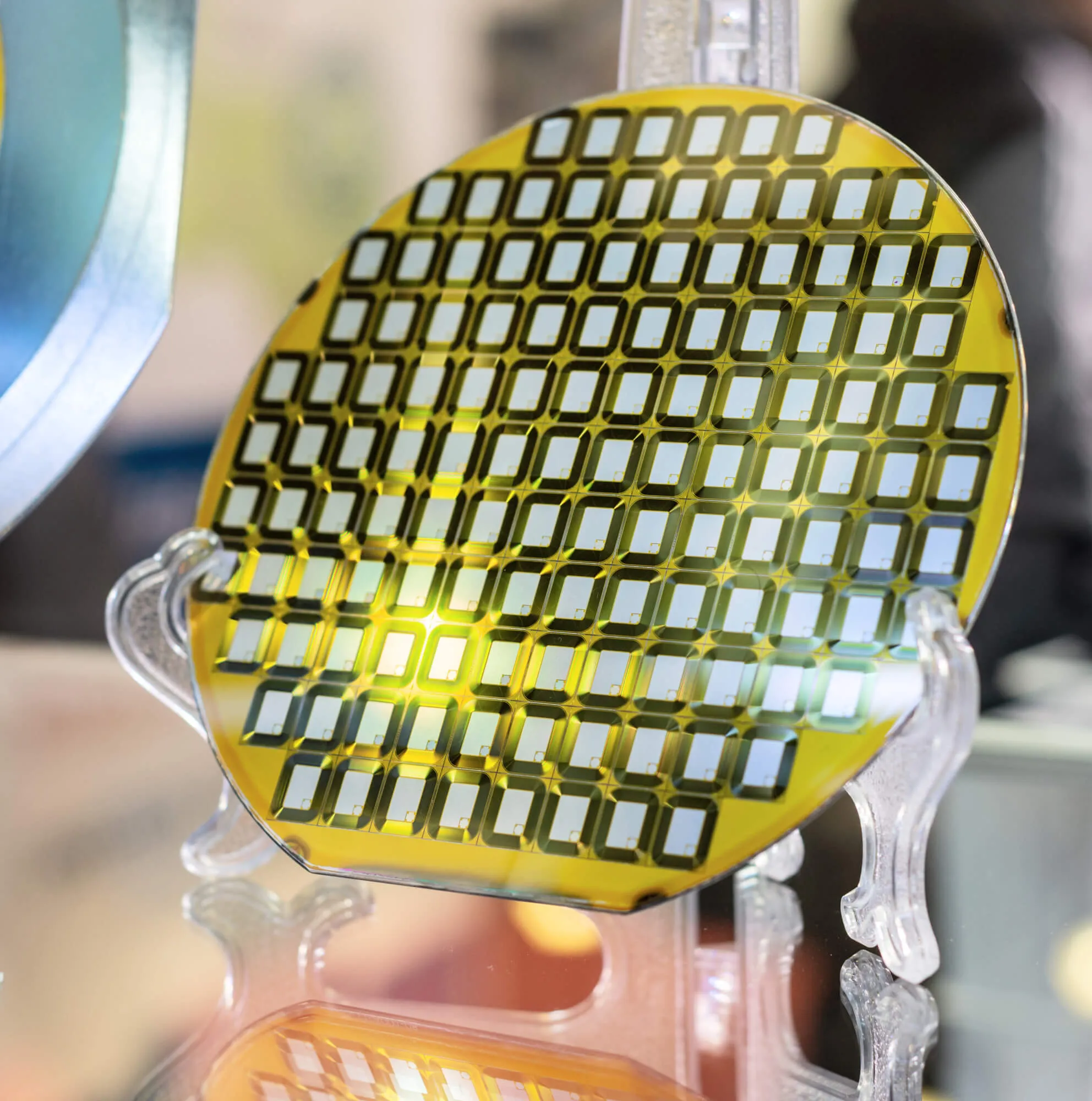
Once we have a fairly pure silicon ingot, now we have to slice it into a wafer. These wafers are very thin and they need to be uniform so the cutting is done with diamond-edged saw blades. Using these blades allows manufacturers to get a fairly thin cut. The diameter of the wafers varies depending on which type of circuits they will be used, naturally, smaller circuitry will require smaller wafers – the largest silicon wafers used for semiconductors are about 12 inches or 300 millimeters.
Silicon wafers conduct tiny amounts of electricity that are highly susceptible to surface structures and variation. Even the smallest of imperfections can diminish the effectiveness of a semiconductor. For this reason, the freshly sliced wafer undergoes a thorough polishing process to achieve a mirror-like surface. Wafers are held in place with a device called a vacuum carrier while they are polished using specially designed pads. The pad is rotated in a downward motion, removing minuscule layers of the wafer until there is no perceivable imperfection and the surface is even and completely flat.

The cleaning process is another key aspect of silicon wafer manufacturing. Tiny particles can cling onto the surface of a silicon wafer and interrupt the flow and transfer of electric currents. Silicon wafer manufacturers must be extremely careful when finishing cleaning the wafers which is why this process takes place in a clean room and requires workers to use specialized gear that helps keep any external particles from finding their way onto the surface of a wafer.
Now that you have a completed wafer, you need to make sure it works well and can withstand the demands of its use. The two biggest hazards for a silicon wafer are electricity and solvents, as these two elements are the leading cause for failure and breakage. To eliminate these hazards, manufacturers put wafers through several tests using computer-controlled probes. These probes test every section of the wafer, if it passes, it’s ready for distribution, if it fails, the silicon wafer is marked and sorted out of the batch.

Wafer World is an industry leader in silicon wafer manufacturing and distribution. If you wish to learn more or want to purchase high quality, expertly made wafer products, we are the ones to call. Contact us today and request a quote!


