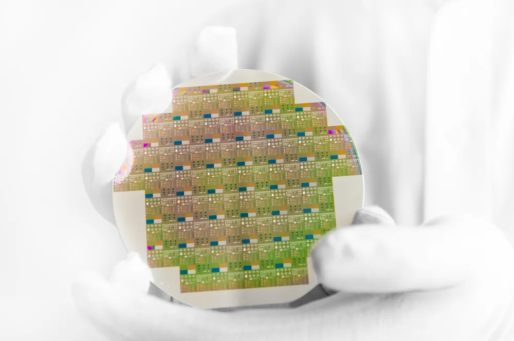
Did you know that a double side polish wafer is integral to most electronic devices? A good semiconductor wafer must be extremely thin and have a shiny finish. Let’s keep reading to learn more about the wafer polishing process!
For starters, wafers must be ground to create a thin and glossy surface. As a result, there is subsurface damage that is visibly present on the wafer itself. A method called, Chemical Mechanical Planarization, refers to the polishing process. During the backgrind process, surface damage is visible on the wafer—and must be removed.
Moreover, silicon wafers are polished by using polishing pads and a liquid diamond substance. The backside of the wafer is held into place with a device called a vacuum carrier. A rotating machine holds a polishing pad and the wafer is brought closer and closer until contact has been made.While the pad is rotating in downward motions, the subsurface damage is removed layer by layer. In effect, a durable silicon wafer is created that is both safe and functional.

Last but not least, we know the importance of getting the best wafer that suits your goals. It should be effective and compatible as a semiconductor. That’s why we are your leaders for creating and supplying the silicon wafer you’ve always wanted. Contact us today to learn more about what we do!


