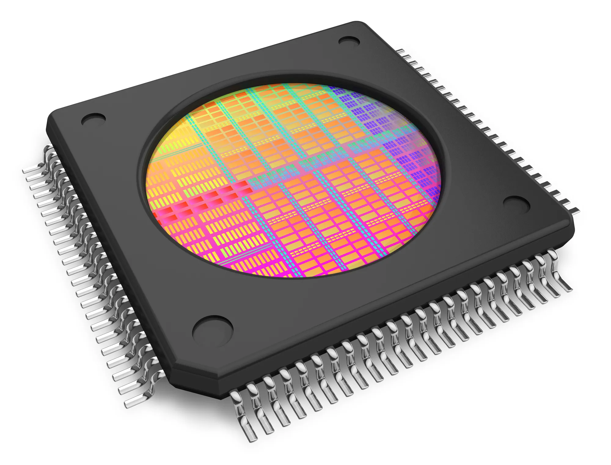
Photolithography is an essential part of silicon wafer processing. This process is focused on etching patterns on the surfaces of silicon and coating them. It utilizes optical radiation to form patterns on a silicon wafer through something known as photoresist layers. Through lithography, millions of devices are created in a large batch. Here are some of the steps involved in the photolithography process:
A liquid polymeric material called a photoresist is coated on a substrate, where the patterns will be imprinted. The coating process happens by spinning the substrate with a speed of 1000-5000 RPM, then the photoresist coating can be poured onto the substrate. This ensures an even coating all over the surface of the substrate. Another alternative process is to use a dry film photoresist and laminate it into place to create a photo-patternable surface.
Using an exposure tool, the photoresist-coated substrate will be exposed. What happens is light will shine through a glass plate, which is partly covered in chrome. This plate, which contains the master image of the device on it, is called photomask or mask. The exposure to light produces a chemical change in the photoresist.
After the exposure step, the substrate will then be submerged in a developer solution. This type of solution breaks down the areas of the photoresist that were caught in the light. The remaining parts that were not dissolved form a pattern which is the master image.
After a Successful Development, the substrate will be subjected to high temperatures between 100-120 degrees Celsius in an oven or hot plate. The goal of this process is to get rid of any liquids absorbed into the substrate and to crosslink the outstanding photoresist. This process improves the mechanical and chemical strength of the material. This prepares it for further silicon wafer processing.

In silicon wafer processing, each process is carefully done to produce the highest quality wafers. If you’re planning to use silicon wafers for your business or next project make sure you get them from Wafer World. Our 22 years of experience in serving our clients excellently has made us no. 1 in the industry. Call us today for any inquiry or purchase the best wafers online!


